Configuração do Kit FPGA

Download do QSF mínimo para: botões, chaves e display (sete segmentos).

Visão Geral

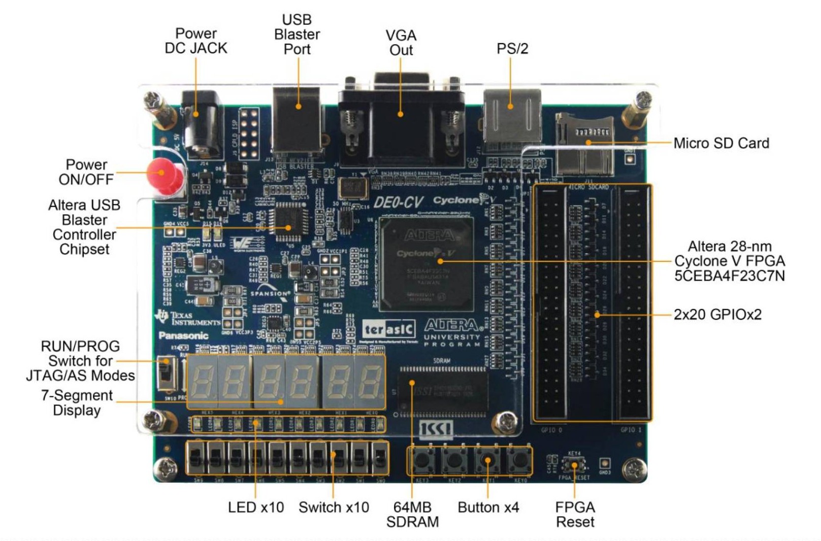
O projeto deve funcionar na placa DE0-CV, portanto, vamos iniciar verificando os recursos disponíveis.

DE0-CV
DE0-CV


Os periféricos do kit de desenvolvimento para FPGA, são conectados ao pinos do chip da FPGA de acordo com o projeto da placa.

Para poder configurar essas conexões, existe um arquivo com a extensão “qsf”. Ele está no diretório do projeto e possui o mesmo nome do projeto.

QSF

Ao criar um novo projeto, o Quartus cria um arquivo nome do projeto.qsf com as definições desse projeto. Porém, nesse momento ele não possui informação sobre quais pinos da FPGA serão utilizados.

É necessário adicionar a definição dos pinos, que serão utilizados, nesse arquivo .qsf. Isso pode ser feito pela edição do arquivo nome do projeto.qsf.

Edição do arquivo nome do projeto.qsf.

Abra o arquivo nome do projeto.qsf e adicione , após o cabeçalho, os conteúdos da listagem: DE0-CV_QSF_minimo.txt.

Os pinos que estão comentados não serão utilizados no curso e podem ser apagados.

Caso não utilize algum outro recurso, comente os seus pinos para evitar mensagens na compilação.

Não sobrescreva o cabeçalho do QSF criado pelo Quartus, adicione, após o cabeçalho, os conteúdos da listagem abaixo.


###Arquivo SDC Mínimo

O arquivo SDC (Synopsis Design Constraint) define os pinos e parâmetros para a verificação da temporização do projeto.

O arquivo está na raíz do diretório do projeto e tem o nome do tipo: “nome do projeto”.sdc

O conteúdo mínimo está abaixo:

# Quartus SDC constraints

# I/Os of the top-level block are called port,
# I/Os of the subblocks are called pin.
# So get_ports and get_pins commands must be used accordingly.
# The signals other than the I/Os are called net.
# The nets may be collected and constrained by using get_nets command, however most of the synthesis tools optimize out them or change the names.
# It is better to avoid using get_nets if not mandatory.
# Otherwise most of the synthesis tools require dont_touch attribute or something similar to keep the net.

# Constrain the main clock:
create_clock -name "CLOCK_50" -period 20.000ns -waveform {0.0 10.0}  [get_ports {CLOCK_50}]

# Constrain the step by step clock (the period may be more than 80 ns but the waveform must be the same):
#create_clock -name "key(0)" -period 80.000ns -waveform {0.0 10.0} [get_ports {key[0]}]

# Constrain the JTAG clock used by In-System Memory Content Editor, SignalTap or Nios II:
#create_clock -period "30.303 ns" -name {altera_reserved_tck} {altera_reserved_tck}

# Only use one of the clocks at a time:
#set_clock_groups -exclusive -group {CLOCK_50} -group {key(0)}

# Constrain the derived clock:
#create_generated_clock -add -source CLOCK_50 -divide_by 62500 -name CLK_400HZ  [get_pins {CLK_400HZ|q}]
#create_generated_clock -add -source [get_pins {CLK_400HZ|q}] -name CLK_10HZ  [get_pins {CLK_10HZ|q}]
#set_false_path -from [get_pins {CLK_400HZ|q}] -to [get_pins {CLK_10HZ|d}]

# Automatically apply a generate clock on the output of phase-locked loops (PLLs)
# This command can be safely left in the SDC even if no PLLs exist in the design
derive_pll_clocks
derive_clock_uncertainty

# Constrain the input I/O path
set_input_delay -clock CLOCK_50 -max 3 [all_inputs]
set_input_delay -clock CLOCK_50 -min 2 [all_inputs]

# Constrain the output I/O path
set_output_delay -clock CLOCK_50 -max 3 [all_outputs]
set_output_delay -clock CLOCK_50 -min 2 [all_outputs]

# Setting LED outputs as false path, since no timing requirement
#set_false_path -from * -to [get_ports LEDR[*]]

# Setting HEX (7 segments) outputs as false path, since no timing requirement
#set_false_path -from * -to [get_ports HEX0[*]]
#set_false_path -from * -to [get_ports HEX1[*]]
#set_false_path -from * -to [get_ports HEX2[*]]
#set_false_path -from * -to [get_ports HEX3[*]]
#set_false_path -from * -to [get_ports HEX4[*]]
#set_false_path -from * -to [get_ports HEX5[*]]

Visão Geral

O projeto deve funcionar na placa DE2-115, portanto, vamos iniciar verificando os recursos disponíveis.

DE2-115
DE2-115


Os periféricos do kit de desenvolvimento para FPGA, são conectados ao pinos do chip da FPGA de acordo com o projeto da placa.

Para poder configurar essas conexões, existe um arquivo com a extensão “qsf”. Ele está no diretório do projeto e possui o mesmo nome do projeto.

Para definir as conexões dos pinos, seus nomes dentro do projeto e suas características elétricas, temos os comandos:

Além disso, é definido o padrão de tensão utilizado nas interfaces:

O limite de corrente:

O tempo de subida (slew rate):

QSF

Abaixo, temos um exemplo do qsf para DE2-115.

Os pinos comentados não serão utilizados no curso.

Caso não utilize algum outro recurso, comente os seus pinos para evitar mensagens na compilação.


#============================================================
# Build by Altera University Program
# FAMILY "Cyclone IV E"
# DEVICE EP4CE115F29C7
#============================================================
#
#
#
# Inicio da config. usada em Design de Computadores
#
#============================================================
# CLOCK
#============================================================
set_location_assignment PIN_Y2 -to CLOCK_50
set_instance_assignment -name IO_STANDARD "3.3-V LVTTL" -to CLOCK_50
#set_location_assignment PIN_AG14 -to CLOCK2_50
#set_instance_assignment -name IO_STANDARD "3.3-V LVTTL" -to CLOCK2_50
#set_location_assignment PIN_AG15 -to CLOCK3_50
#set_instance_assignment -name IO_STANDARD "3.3-V LVTTL" -to CLOCK3_50

#============================================================
# LED
#============================================================
set_location_assignment PIN_E21 -to LEDG[0]
set_location_assignment PIN_E22 -to LEDG[1]
set_location_assignment PIN_E25 -to LEDG[2]
set_location_assignment PIN_E24 -to LEDG[3]
set_location_assignment PIN_H21 -to LEDG[4]
set_location_assignment PIN_G20 -to LEDG[5]
set_location_assignment PIN_G22 -to LEDG[6]
set_location_assignment PIN_G21 -to LEDG[7]
set_location_assignment PIN_F17 -to LEDG[8]
set_instance_assignment -name IO_STANDARD "2.5 V" -to LEDG[0]
set_instance_assignment -name IO_STANDARD "2.5 V" -to LEDG[1]
set_instance_assignment -name IO_STANDARD "2.5 V" -to LEDG[2]
set_instance_assignment -name IO_STANDARD "2.5 V" -to LEDG[3]
set_instance_assignment -name IO_STANDARD "2.5 V" -to LEDG[4]
set_instance_assignment -name IO_STANDARD "2.5 V" -to LEDG[5]
set_instance_assignment -name IO_STANDARD "2.5 V" -to LEDG[6]
set_instance_assignment -name IO_STANDARD "2.5 V" -to LEDG[7]
set_instance_assignment -name IO_STANDARD "2.5 V" -to LEDG[8]
#
set_instance_assignment -name SLEW_RATE 2 -to LEDG
set_instance_assignment -name CURRENT_STRENGTH_NEW DEFAULT -to LEDG
#
set_location_assignment PIN_G19 -to LEDR[0]
set_location_assignment PIN_E19 -to LEDR[2]
set_location_assignment PIN_F19 -to LEDR[1]
set_location_assignment PIN_F21 -to LEDR[3]
set_location_assignment PIN_F18 -to LEDR[4]
set_location_assignment PIN_E18 -to LEDR[5]
set_location_assignment PIN_J19 -to LEDR[6]
set_location_assignment PIN_H19 -to LEDR[7]
set_location_assignment PIN_J17 -to LEDR[8]
set_location_assignment PIN_G17 -to LEDR[9]
set_location_assignment PIN_J15 -to LEDR[10]
set_location_assignment PIN_H16 -to LEDR[11]
set_location_assignment PIN_J16 -to LEDR[12]
set_location_assignment PIN_H17 -to LEDR[13]
set_location_assignment PIN_F15 -to LEDR[14]
set_location_assignment PIN_G15 -to LEDR[15]
set_location_assignment PIN_G16 -to LEDR[16]
set_location_assignment PIN_H15 -to LEDR[17]
set_instance_assignment -name IO_STANDARD "2.5 V" -to LEDR[0]
set_instance_assignment -name IO_STANDARD "2.5 V" -to LEDR[1]
set_instance_assignment -name IO_STANDARD "2.5 V" -to LEDR[2]
set_instance_assignment -name IO_STANDARD "2.5 V" -to LEDR[3]
set_instance_assignment -name IO_STANDARD "2.5 V" -to LEDR[4]
set_instance_assignment -name IO_STANDARD "2.5 V" -to LEDR[5]
set_instance_assignment -name IO_STANDARD "2.5 V" -to LEDR[6]
set_instance_assignment -name IO_STANDARD "2.5 V" -to LEDR[7]
set_instance_assignment -name IO_STANDARD "2.5 V" -to LEDR[8]
set_instance_assignment -name IO_STANDARD "2.5 V" -to LEDR[9]
set_instance_assignment -name IO_STANDARD "2.5 V" -to LEDR[10]
set_instance_assignment -name IO_STANDARD "2.5 V" -to LEDR[11]
set_instance_assignment -name IO_STANDARD "2.5 V" -to LEDR[12]
set_instance_assignment -name IO_STANDARD "2.5 V" -to LEDR[13]
set_instance_assignment -name IO_STANDARD "2.5 V" -to LEDR[14]
set_instance_assignment -name IO_STANDARD "2.5 V" -to LEDR[15]
set_instance_assignment -name IO_STANDARD "2.5 V" -to LEDR[16]
set_instance_assignment -name IO_STANDARD "2.5 V" -to LEDR[17]
#
set_instance_assignment -name SLEW_RATE 2 -to LEDR
set_instance_assignment -name CURRENT_STRENGTH_NEW DEFAULT -to LEDR

#============================================================
# KEY
#============================================================
set_location_assignment PIN_M23 -to KEY[0]
set_location_assignment PIN_M21 -to KEY[1]
set_location_assignment PIN_N21 -to KEY[2]
set_location_assignment PIN_R24 -to KEY[3]
set_instance_assignment -name IO_STANDARD "2.5 V" -to KEY[0]
set_instance_assignment -name IO_STANDARD "2.5 V" -to KEY[1]
set_instance_assignment -name IO_STANDARD "2.5 V" -to KEY[2]
set_instance_assignment -name IO_STANDARD "2.5 V" -to KEY[3]
set_instance_assignment -name IO_MAXIMUM_TOGGLE_RATE "0 MHz" -to KEY

#============================================================
# SW
#============================================================
set_location_assignment PIN_AB28 -to SW[0]
set_location_assignment PIN_AC28 -to SW[1]
set_location_assignment PIN_AC27 -to SW[2]
set_location_assignment PIN_AD27 -to SW[3]
set_location_assignment PIN_AB27 -to SW[4]
set_location_assignment PIN_AC26 -to SW[5]
set_location_assignment PIN_AD26 -to SW[6]
set_location_assignment PIN_AB26 -to SW[7]
set_location_assignment PIN_AC25 -to SW[8]
set_location_assignment PIN_AB25 -to SW[9]
set_location_assignment PIN_AC24 -to SW[10]
set_location_assignment PIN_AB24 -to SW[11]
set_location_assignment PIN_AB23 -to SW[12]
set_location_assignment PIN_AA24 -to SW[13]
set_location_assignment PIN_AA23 -to SW[14]
set_location_assignment PIN_AA22 -to SW[15]
set_location_assignment PIN_Y24 -to SW[16]
set_location_assignment PIN_Y23 -to SW[17]
set_instance_assignment -name IO_STANDARD "2.5 V" -to SW[0]
set_instance_assignment -name IO_STANDARD "2.5 V" -to SW[1]
set_instance_assignment -name IO_STANDARD "2.5 V" -to SW[2]
set_instance_assignment -name IO_STANDARD "2.5 V" -to SW[3]
set_instance_assignment -name IO_STANDARD "2.5 V" -to SW[4]
set_instance_assignment -name IO_STANDARD "2.5 V" -to SW[5]
set_instance_assignment -name IO_STANDARD "2.5 V" -to SW[6]
set_instance_assignment -name IO_STANDARD "2.5 V" -to SW[7]
set_instance_assignment -name IO_STANDARD "2.5 V" -to SW[8]
set_instance_assignment -name IO_STANDARD "2.5 V" -to SW[9]
set_instance_assignment -name IO_STANDARD "2.5 V" -to SW[10]
set_instance_assignment -name IO_STANDARD "2.5 V" -to SW[11]
set_instance_assignment -name IO_STANDARD "2.5 V" -to SW[12]
set_instance_assignment -name IO_STANDARD "2.5 V" -to SW[13]
set_instance_assignment -name IO_STANDARD "2.5 V" -to SW[14]
set_instance_assignment -name IO_STANDARD "2.5 V" -to SW[15]
set_instance_assignment -name IO_STANDARD "2.5 V" -to SW[16]
set_instance_assignment -name IO_STANDARD "2.5 V" -to SW[17]
set_instance_assignment -name IO_MAXIMUM_TOGGLE_RATE "0 MHz" -to SW

#============================================================
# SEG7
#============================================================
set_location_assignment PIN_G18 -to HEX0[0]
set_location_assignment PIN_F22 -to HEX0[1]
set_location_assignment PIN_E17 -to HEX0[2]
set_location_assignment PIN_L26 -to HEX0[3]
set_location_assignment PIN_L25 -to HEX0[4]
set_location_assignment PIN_J22 -to HEX0[5]
set_location_assignment PIN_H22 -to HEX0[6]
set_location_assignment PIN_M24 -to HEX1[0]
set_location_assignment PIN_Y22 -to HEX1[1]
set_location_assignment PIN_W21 -to HEX1[2]
set_location_assignment PIN_W22 -to HEX1[3]
set_location_assignment PIN_W25 -to HEX1[4]
set_location_assignment PIN_U23 -to HEX1[5]
set_location_assignment PIN_U24 -to HEX1[6]
set_location_assignment PIN_AA25 -to HEX2[0]
set_location_assignment PIN_AA26 -to HEX2[1]
set_location_assignment PIN_Y25 -to HEX2[2]
set_location_assignment PIN_W26 -to HEX2[3]
set_location_assignment PIN_Y26 -to HEX2[4]
set_location_assignment PIN_W27 -to HEX2[5]
set_location_assignment PIN_W28 -to HEX2[6]
set_location_assignment PIN_V21 -to HEX3[0]
set_location_assignment PIN_U21 -to HEX3[1]
set_location_assignment PIN_AB20 -to HEX3[2]
set_location_assignment PIN_AA21 -to HEX3[3]
set_location_assignment PIN_AD24 -to HEX3[4]
set_location_assignment PIN_AF23 -to HEX3[5]
set_location_assignment PIN_Y19 -to HEX3[6]
set_location_assignment PIN_AB19 -to HEX4[0]
set_location_assignment PIN_AA19 -to HEX4[1]
set_location_assignment PIN_AG21 -to HEX4[2]
set_location_assignment PIN_AH21 -to HEX4[3]
set_location_assignment PIN_AE19 -to HEX4[4]
set_location_assignment PIN_AF19 -to HEX4[5]
set_location_assignment PIN_AE18 -to HEX4[6]
set_location_assignment PIN_AD18 -to HEX5[0]
set_location_assignment PIN_AC18 -to HEX5[1]
set_location_assignment PIN_AB18 -to HEX5[2]
set_location_assignment PIN_AH19 -to HEX5[3]
set_location_assignment PIN_AG19 -to HEX5[4]
set_location_assignment PIN_AF18 -to HEX5[5]
set_location_assignment PIN_AH18 -to HEX5[6]
set_location_assignment PIN_AA17 -to HEX6[0]
set_location_assignment PIN_AB16 -to HEX6[1]
set_location_assignment PIN_AA16 -to HEX6[2]
set_location_assignment PIN_AB17 -to HEX6[3]
set_location_assignment PIN_AB15 -to HEX6[4]
set_location_assignment PIN_AA15 -to HEX6[5]
set_location_assignment PIN_AC17 -to HEX6[6]
set_location_assignment PIN_AD17 -to HEX7[0]
set_location_assignment PIN_AE17 -to HEX7[1]
set_location_assignment PIN_AG17 -to HEX7[2]
set_location_assignment PIN_AH17 -to HEX7[3]
set_location_assignment PIN_AF17 -to HEX7[4]
set_location_assignment PIN_AG18 -to HEX7[5]
set_location_assignment PIN_AA14 -to HEX7[6]
set_instance_assignment -name IO_STANDARD "2.5 V" -to HEX0[0]
set_instance_assignment -name IO_STANDARD "2.5 V" -to HEX0[1]
set_instance_assignment -name IO_STANDARD "2.5 V" -to HEX0[2]
set_instance_assignment -name IO_STANDARD "2.5 V" -to HEX0[3]
set_instance_assignment -name IO_STANDARD "2.5 V" -to HEX0[4]
set_instance_assignment -name IO_STANDARD "2.5 V" -to HEX0[5]
set_instance_assignment -name IO_STANDARD "2.5 V" -to HEX0[6]
set_instance_assignment -name IO_STANDARD "2.5 V" -to HEX1[0]
set_instance_assignment -name IO_STANDARD "2.5 V" -to HEX1[1]
set_instance_assignment -name IO_STANDARD "2.5 V" -to HEX1[2]
set_instance_assignment -name IO_STANDARD "2.5 V" -to HEX1[3]
set_instance_assignment -name IO_STANDARD "2.5 V" -to HEX1[4]
set_instance_assignment -name IO_STANDARD "2.5 V" -to HEX1[5]
set_instance_assignment -name IO_STANDARD "2.5 V" -to HEX1[6]
set_instance_assignment -name IO_STANDARD "2.5 V" -to HEX2[0]
set_instance_assignment -name IO_STANDARD "2.5 V" -to HEX2[1]
set_instance_assignment -name IO_STANDARD "2.5 V" -to HEX2[2]
set_instance_assignment -name IO_STANDARD "2.5 V" -to HEX2[3]
set_instance_assignment -name IO_STANDARD "2.5 V" -to HEX2[4]
set_instance_assignment -name IO_STANDARD "2.5 V" -to HEX2[5]
set_instance_assignment -name IO_STANDARD "2.5 V" -to HEX2[6]
set_instance_assignment -name IO_STANDARD "2.5 V" -to HEX3[0]
set_instance_assignment -name IO_STANDARD "2.5 V" -to HEX3[1]
set_instance_assignment -name IO_STANDARD "3.3-V LVTTL" -to HEX3[2]
set_instance_assignment -name IO_STANDARD "3.3-V LVTTL" -to HEX3[3]
set_instance_assignment -name IO_STANDARD "3.3-V LVTTL" -to HEX3[4]
set_instance_assignment -name IO_STANDARD "3.3-V LVTTL" -to HEX3[5]
set_instance_assignment -name IO_STANDARD "3.3-V LVTTL" -to HEX3[6]
set_instance_assignment -name IO_STANDARD "3.3-V LVTTL" -to HEX4[0]
set_instance_assignment -name IO_STANDARD "3.3-V LVTTL" -to HEX4[1]
set_instance_assignment -name IO_STANDARD "3.3-V LVTTL" -to HEX4[2]
set_instance_assignment -name IO_STANDARD "3.3-V LVTTL" -to HEX4[3]
set_instance_assignment -name IO_STANDARD "3.3-V LVTTL" -to HEX4[4]
set_instance_assignment -name IO_STANDARD "3.3-V LVTTL" -to HEX4[5]
set_instance_assignment -name IO_STANDARD "3.3-V LVTTL" -to HEX4[6]
set_instance_assignment -name IO_STANDARD "3.3-V LVTTL" -to HEX5[0]
set_instance_assignment -name IO_STANDARD "3.3-V LVTTL" -to HEX5[1]
set_instance_assignment -name IO_STANDARD "3.3-V LVTTL" -to HEX5[2]
set_instance_assignment -name IO_STANDARD "3.3-V LVTTL" -to HEX5[3]
set_instance_assignment -name IO_STANDARD "3.3-V LVTTL" -to HEX5[4]
set_instance_assignment -name IO_STANDARD "3.3-V LVTTL" -to HEX5[5]
set_instance_assignment -name IO_STANDARD "3.3-V LVTTL" -to HEX5[6]
set_instance_assignment -name IO_STANDARD "3.3-V LVTTL" -to HEX6[0]
set_instance_assignment -name IO_STANDARD "3.3-V LVTTL" -to HEX6[1]
set_instance_assignment -name IO_STANDARD "3.3-V LVTTL" -to HEX6[2]
set_instance_assignment -name IO_STANDARD "3.3-V LVTTL" -to HEX6[3]
set_instance_assignment -name IO_STANDARD "3.3-V LVTTL" -to HEX6[4]
set_instance_assignment -name IO_STANDARD "3.3-V LVTTL" -to HEX6[5]
set_instance_assignment -name IO_STANDARD "3.3-V LVTTL" -to HEX6[6]
set_instance_assignment -name IO_STANDARD "3.3-V LVTTL" -to HEX7[0]
set_instance_assignment -name IO_STANDARD "3.3-V LVTTL" -to HEX7[1]
set_instance_assignment -name IO_STANDARD "3.3-V LVTTL" -to HEX7[2]
set_instance_assignment -name IO_STANDARD "3.3-V LVTTL" -to HEX7[3]
set_instance_assignment -name IO_STANDARD "3.3-V LVTTL" -to HEX7[4]
set_instance_assignment -name IO_STANDARD "3.3-V LVTTL" -to HEX7[5]
set_instance_assignment -name IO_STANDARD "3.3-V LVTTL" -to HEX7[6]

set_instance_assignment -name SLEW_RATE 2 -to HEX0
set_instance_assignment -name SLEW_RATE 2 -to HEX1
set_instance_assignment -name SLEW_RATE 2 -to HEX2
set_instance_assignment -name SLEW_RATE 2 -to HEX3
set_instance_assignment -name SLEW_RATE 2 -to HEX4
set_instance_assignment -name SLEW_RATE 2 -to HEX5
set_instance_assignment -name SLEW_RATE 2 -to HEX6
set_instance_assignment -name SLEW_RATE 2 -to HEX7


set_instance_assignment -name CURRENT_STRENGTH_NEW DEFAULT -to HEX0
set_instance_assignment -name CURRENT_STRENGTH_NEW DEFAULT -to HEX1
set_instance_assignment -name CURRENT_STRENGTH_NEW DEFAULT -to HEX2
set_instance_assignment -name CURRENT_STRENGTH_NEW DEFAULT -to HEX3
set_instance_assignment -name CURRENT_STRENGTH_NEW DEFAULT -to HEX4
set_instance_assignment -name CURRENT_STRENGTH_NEW DEFAULT -to HEX5
set_instance_assignment -name CURRENT_STRENGTH_NEW DEFAULT -to HEX6
set_instance_assignment -name CURRENT_STRENGTH_NEW DEFAULT -to HEX7

set_instance_assignment -name IO_MAXIMUM_TOGGLE_RATE "0 MHz" -to HEX0
set_instance_assignment -name IO_MAXIMUM_TOGGLE_RATE "0 MHz" -to HEX1
set_instance_assignment -name IO_MAXIMUM_TOGGLE_RATE "0 MHz" -to HEX2
set_instance_assignment -name IO_MAXIMUM_TOGGLE_RATE "0 MHz" -to HEX3
set_instance_assignment -name IO_MAXIMUM_TOGGLE_RATE "0 MHz" -to HEX4
set_instance_assignment -name IO_MAXIMUM_TOGGLE_RATE "0 MHz" -to HEX5
set_instance_assignment -name IO_MAXIMUM_TOGGLE_RATE "0 MHz" -to HEX6
set_instance_assignment -name IO_MAXIMUM_TOGGLE_RATE "0 MHz" -to HEX7


#
#
# Fim da config. utilizada em Design de Computadores
#
#
#
#============================================================
#============================================================
#============================================================
#============================================================
#
#============================================================
# Sma
#============================================================
#set_location_assignment PIN_AH14 -to SMA_CLKIN
#set_location_assignment PIN_AE23 -to SMA_CLKOUT
#set_instance_assignment -name IO_STANDARD "3.3-V LVTTL" -to SMA_CLKIN
#set_instance_assignment -name IO_STANDARD "3.3-V LVTTL" -to SMA_CLKOUT

#============================================================
# LCD
#============================================================
#set_location_assignment PIN_L6 -to LCD_BLON
#set_location_assignment PIN_M5 -to LCD_DATA[7]
#set_location_assignment PIN_M3 -to LCD_DATA[6]
#set_location_assignment PIN_K2 -to LCD_DATA[5]
#set_location_assignment PIN_K1 -to LCD_DATA[4]
#set_location_assignment PIN_K7 -to LCD_DATA[3]
#set_location_assignment PIN_L2 -to LCD_DATA[2]
#set_location_assignment PIN_L1 -to LCD_DATA[1]
#set_location_assignment PIN_L3 -to LCD_DATA[0]
#set_location_assignment PIN_L4 -to LCD_EN
#set_location_assignment PIN_M1 -to LCD_RW
#set_location_assignment PIN_M2 -to LCD_RS
#set_location_assignment PIN_L5 -to LCD_ON
#set_instance_assignment -name IO_STANDARD "3.3-V LVTTL" -to LCD_DATA[0]
#set_instance_assignment -name IO_STANDARD "3.3-V LVTTL" -to LCD_DATA[1]
#set_instance_assignment -name IO_STANDARD "3.3-V LVTTL" -to LCD_DATA[2]
#set_instance_assignment -name IO_STANDARD "3.3-V LVTTL" -to LCD_DATA[3]
#set_instance_assignment -name IO_STANDARD "3.3-V LVTTL" -to LCD_DATA[4]
#set_instance_assignment -name IO_STANDARD "3.3-V LVTTL" -to LCD_DATA[5]
#set_instance_assignment -name IO_STANDARD "3.3-V LVTTL" -to LCD_DATA[6]
#set_instance_assignment -name IO_STANDARD "3.3-V LVTTL" -to LCD_DATA[7]
#set_instance_assignment -name IO_STANDARD "3.3-V LVTTL" -to LCD_BLON
#set_instance_assignment -name IO_STANDARD "3.3-V LVTTL" -to LCD_RW
#set_instance_assignment -name IO_STANDARD "3.3-V LVTTL" -to LCD_EN
#set_instance_assignment -name IO_STANDARD "3.3-V LVTTL" -to LCD_RS
#set_instance_assignment -name IO_STANDARD "3.3-V LVTTL" -to LCD_ON

#============================================================
# RS232
#============================================================
#set_location_assignment PIN_G9 -to UART_TXD
#set_location_assignment PIN_G12 -to UART_RXD
#set_location_assignment PIN_G14 -to UART_CTS
#set_location_assignment PIN_J13 -to UART_RTS
#set_instance_assignment -name IO_STANDARD "3.3-V LVTTL" -to UART_TXD
#set_instance_assignment -name IO_STANDARD "3.3-V LVTTL" -to UART_RXD
#set_instance_assignment -name IO_STANDARD "3.3-V LVTTL" -to UART_CTS
#set_instance_assignment -name IO_STANDARD "3.3-V LVTTL" -to UART_RTS

#============================================================
# PS2
#============================================================
#set_location_assignment PIN_G6 -to PS2_KBCLK
#set_location_assignment PIN_H5 -to PS2_KBDAT
#set_location_assignment PIN_G5 -to PS2_MSCLK
#set_location_assignment PIN_F5 -to PS2_MSDAT
#set_instance_assignment -name IO_STANDARD "3.3-V LVTTL" -to PS2_KBCLK
#set_instance_assignment -name IO_STANDARD "3.3-V LVTTL" -to PS2_KBDAT
#set_instance_assignment -name IO_STANDARD "3.3-V LVTTL" -to PS2_MSCLK
#set_instance_assignment -name IO_STANDARD "3.3-V LVTTL" -to PS2_MSDAT

#============================================================
# SDCARD
#============================================================
#set_location_assignment PIN_AE14 -to SD_DAT[0]
#set_location_assignment PIN_AF13 -to SD_DAT[1]
#set_location_assignment PIN_AB14 -to SD_DAT[2]
#set_location_assignment PIN_AC14 -to SD_DAT[3]
#set_location_assignment PIN_AE13 -to SD_CLK
#set_location_assignment PIN_AD14 -to SD_CMD
#set_location_assignment PIN_AF14 -to SD_WP_N
#set_instance_assignment -name IO_STANDARD "3.3-V LVTTL" -to SD_CMD
#set_instance_assignment -name IO_STANDARD "3.3-V LVTTL" -to SD_CLK
#set_instance_assignment -name IO_STANDARD "3.3-V LVTTL" -to SD_WP_N
#set_instance_assignment -name IO_STANDARD "3.3-V LVTTL" -to SD_DAT[0]
#set_instance_assignment -name IO_STANDARD "3.3-V LVTTL" -to SD_DAT[1]
#set_instance_assignment -name IO_STANDARD "3.3-V LVTTL" -to SD_DAT[2]
#set_instance_assignment -name IO_STANDARD "3.3-V LVTTL" -to SD_DAT[3]

#============================================================
# VGA
#============================================================
#set_location_assignment PIN_D12 -to VGA_B[7]
#set_location_assignment PIN_D11 -to VGA_B[6]
#set_location_assignment PIN_C12 -to VGA_B[5]
#set_location_assignment PIN_A11 -to VGA_B[4]
#set_location_assignment PIN_B11 -to VGA_B[3]
#set_location_assignment PIN_C11 -to VGA_B[2]
#set_location_assignment PIN_A10 -to VGA_B[1]
#set_location_assignment PIN_B10 -to VGA_B[0]
#set_location_assignment PIN_C9 -to VGA_G[7]
#set_location_assignment PIN_F10 -to VGA_G[6]
#set_location_assignment PIN_B8 -to VGA_G[5]
#set_location_assignment PIN_C8 -to VGA_G[4]
#set_location_assignment PIN_H12 -to VGA_G[3]
#set_location_assignment PIN_F8 -to VGA_G[2]
#set_location_assignment PIN_G11 -to VGA_G[1]
#set_location_assignment PIN_G8 -to VGA_G[0]
#set_location_assignment PIN_H10 -to VGA_R[7]
#set_location_assignment PIN_H8 -to VGA_R[6]
#set_location_assignment PIN_J12 -to VGA_R[5]
#set_location_assignment PIN_G10 -to VGA_R[4]
#set_location_assignment PIN_F12 -to VGA_R[3]
#set_location_assignment PIN_D10 -to VGA_R[2]
#set_location_assignment PIN_E11 -to VGA_R[1]
#set_location_assignment PIN_E12 -to VGA_R[0]
#set_location_assignment PIN_A12 -to VGA_CLK
#set_location_assignment PIN_F11 -to VGA_BLANK_N
#set_location_assignment PIN_C10 -to VGA_SYNC_N
#set_location_assignment PIN_G13 -to VGA_HS
#set_location_assignment PIN_C13 -to VGA_VS
#set_instance_assignment -name IO_STANDARD "3.3-V LVTTL" -to VGA_HS
#set_instance_assignment -name IO_STANDARD "3.3-V LVTTL" -to VGA_VS
#set_instance_assignment -name IO_STANDARD "3.3-V LVTTL" -to VGA_SYNC_N
#set_instance_assignment -name IO_STANDARD "3.3-V LVTTL" -to VGA_CLK
#set_instance_assignment -name IO_STANDARD "3.3-V LVTTL" -to VGA_BLANK_N
#set_instance_assignment -name IO_STANDARD "3.3-V LVTTL" -to VGA_R[0]
#set_instance_assignment -name IO_STANDARD "3.3-V LVTTL" -to VGA_R[1]
#set_instance_assignment -name IO_STANDARD "3.3-V LVTTL" -to VGA_R[2]
#set_instance_assignment -name IO_STANDARD "3.3-V LVTTL" -to VGA_R[3]
#set_instance_assignment -name IO_STANDARD "3.3-V LVTTL" -to VGA_R[4]
#set_instance_assignment -name IO_STANDARD "3.3-V LVTTL" -to VGA_R[5]
#set_instance_assignment -name IO_STANDARD "3.3-V LVTTL" -to VGA_R[6]
#set_instance_assignment -name IO_STANDARD "3.3-V LVTTL" -to VGA_R[7]
#set_instance_assignment -name IO_STANDARD "3.3-V LVTTL" -to VGA_G[0]
#set_instance_assignment -name IO_STANDARD "3.3-V LVTTL" -to VGA_G[1]
#set_instance_assignment -name IO_STANDARD "3.3-V LVTTL" -to VGA_G[2]
#set_instance_assignment -name IO_STANDARD "3.3-V LVTTL" -to VGA_G[3]
#set_instance_assignment -name IO_STANDARD "3.3-V LVTTL" -to VGA_G[4]
#set_instance_assignment -name IO_STANDARD "3.3-V LVTTL" -to VGA_G[5]
#set_instance_assignment -name IO_STANDARD "3.3-V LVTTL" -to VGA_G[6]
#set_instance_assignment -name IO_STANDARD "3.3-V LVTTL" -to VGA_G[7]
#set_instance_assignment -name IO_STANDARD "3.3-V LVTTL" -to VGA_B[0]
#set_instance_assignment -name IO_STANDARD "3.3-V LVTTL" -to VGA_B[1]
#set_instance_assignment -name IO_STANDARD "3.3-V LVTTL" -to VGA_B[2]
#set_instance_assignment -name IO_STANDARD "3.3-V LVTTL" -to VGA_B[3]
#set_instance_assignment -name IO_STANDARD "3.3-V LVTTL" -to VGA_B[4]
#set_instance_assignment -name IO_STANDARD "3.3-V LVTTL" -to VGA_B[5]
#set_instance_assignment -name IO_STANDARD "3.3-V LVTTL" -to VGA_B[6]
#set_instance_assignment -name IO_STANDARD "3.3-V LVTTL" -to VGA_B[7]

#============================================================
# Audio
#============================================================
#set_location_assignment PIN_D1 -to AUD_DACDAT
#set_location_assignment PIN_E3 -to AUD_DACLRCK
#set_location_assignment PIN_D2 -to AUD_ADCDAT
#set_location_assignment PIN_C2 -to AUD_ADCLRCK
#set_location_assignment PIN_E1 -to AUD_XCK
#set_location_assignment PIN_F2 -to AUD_BCLK
#set_instance_assignment -name IO_STANDARD "3.3-V LVTTL" -to AUD_ADCLRCK
#set_instance_assignment -name IO_STANDARD "3.3-V LVTTL" -to AUD_ADCDAT
#set_instance_assignment -name IO_STANDARD "3.3-V LVTTL" -to AUD_DACLRCK
#set_instance_assignment -name IO_STANDARD "3.3-V LVTTL" -to AUD_DACDAT
#set_instance_assignment -name IO_STANDARD "3.3-V LVTTL" -to AUD_XCK
#set_instance_assignment -name IO_STANDARD "3.3-V LVTTL" -to AUD_BCLK

#============================================================
# I2C for EEPROM
#============================================================
#set_location_assignment PIN_D14 -to EEP_I2C_SCLK
#set_location_assignment PIN_E14 -to EEP_I2C_SDAT
#set_instance_assignment -name IO_STANDARD "3.3-V LVTTL" -to EEP_I2C_SCLK
#set_instance_assignment -name IO_STANDARD "3.3-V LVTTL" -to EEP_I2C_SDAT

#============================================================
# I2C for Audioand Tv-Decode 1 and 2
#============================================================
#set_location_assignment PIN_B7 -to I2C_SCLK
#set_location_assignment PIN_A8 -to I2C_SDAT
#set_instance_assignment -name IO_STANDARD "3.3-V LVTTL" -to I2C_SCLK
#set_instance_assignment -name IO_STANDARD "3.3-V LVTTL" -to I2C_SDAT

#============================================================
# Ethernet 0
#============================================================
#set_location_assignment PIN_A17 -to ENET0_GTX_CLK
#set_location_assignment PIN_A21 -to ENET0_INT_N
#set_location_assignment PIN_C20 -to ENET0_MDC
#set_location_assignment PIN_B21 -to ENET0_MDIO
#set_location_assignment PIN_C19 -to ENET0_RESET_N
#set_location_assignment PIN_A15 -to ENET0_RX_CLK
#set_location_assignment PIN_E15 -to ENET0_RX_COL
#set_location_assignment PIN_D15 -to ENET0_RX_CRS
#set_location_assignment PIN_C16 -to ENET0_RX_DATA[0]
#set_location_assignment PIN_D16 -to ENET0_RX_DATA[1]
#set_location_assignment PIN_D17 -to ENET0_RX_DATA[2]
#set_location_assignment PIN_C15 -to ENET0_RX_DATA[3]
#set_location_assignment PIN_C17 -to ENET0_RX_DV
#set_location_assignment PIN_D18 -to ENET0_RX_ER
#set_location_assignment PIN_B17 -to ENET0_TX_CLK
#set_location_assignment PIN_C18 -to ENET0_TX_DATA[0]
#set_location_assignment PIN_D19 -to ENET0_TX_DATA[1]
#set_location_assignment PIN_A19 -to ENET0_TX_DATA[2]
#set_location_assignment PIN_B19 -to ENET0_TX_DATA[3]
#set_location_assignment PIN_A18 -to ENET0_TX_EN
#set_location_assignment PIN_B18 -to ENET0_TX_ER
#set_instance_assignment -name IO_STANDARD "2.5 V" -to ENET0_TX_DATA[0]
#set_instance_assignment -name IO_STANDARD "2.5 V" -to ENET0_RX_DATA[0]
#set_instance_assignment -name IO_STANDARD "2.5 V" -to ENET0_TX_DATA[1]
#set_instance_assignment -name IO_STANDARD "2.5 V" -to ENET0_RX_DATA[1]
#set_instance_assignment -name IO_STANDARD "2.5 V" -to ENET0_TX_DATA[2]
#set_instance_assignment -name IO_STANDARD "2.5 V" -to ENET0_RX_DATA[2]
#set_instance_assignment -name IO_STANDARD "2.5 V" -to ENET0_TX_DATA[3]
#set_instance_assignment -name IO_STANDARD "2.5 V" -to ENET0_RX_DATA[3]
#set_instance_assignment -name IO_STANDARD "2.5 V" -to ENET0_GTX_CLK
#set_instance_assignment -name IO_STANDARD "2.5 V" -to ENET0_TX_EN
#set_instance_assignment -name IO_STANDARD "2.5 V" -to ENET0_TX_ER
#set_instance_assignment -name IO_STANDARD "2.5 V" -to ENET0_INT_N
#set_instance_assignment -name IO_STANDARD "2.5 V" -to ENET0_RESET_N
#set_instance_assignment -name IO_STANDARD "2.5 V" -to ENET0_RX_DV
#set_instance_assignment -name IO_STANDARD "2.5 V" -to ENET0_RX_ER
#set_instance_assignment -name IO_STANDARD "2.5 V" -to ENET0_RX_CRS
#set_instance_assignment -name IO_STANDARD "2.5 V" -to ENET0_RX_COL
#set_instance_assignment -name IO_STANDARD "2.5 V" -to ENET0_RX_CLK
#set_instance_assignment -name IO_STANDARD "2.5 V" -to ENET0_TX_CLK
#set_instance_assignment -name IO_STANDARD "2.5 V" -to ENET0_MDC
#set_instance_assignment -name IO_STANDARD "2.5 V" -to ENET0_MDIO

#============================================================
# Ethernet 1
#============================================================
#set_location_assignment PIN_C23 -to ENET1_GTX_CLK
#set_location_assignment PIN_D24 -to ENET1_INT_N
#set_location_assignment PIN_D23 -to ENET1_MDC
#set_location_assignment PIN_D25 -to ENET1_MDIO
#set_location_assignment PIN_D22 -to ENET1_RESET_N
#set_location_assignment PIN_B15 -to ENET1_RX_CLK
#set_location_assignment PIN_B22 -to ENET1_RX_COL
#set_location_assignment PIN_D20 -to ENET1_RX_CRS
#set_location_assignment PIN_B23 -to ENET1_RX_DATA[0]
#set_location_assignment PIN_C21 -to ENET1_RX_DATA[1]
#set_location_assignment PIN_A23 -to ENET1_RX_DATA[2]
#set_location_assignment PIN_D21 -to ENET1_RX_DATA[3]
#set_location_assignment PIN_A22 -to ENET1_RX_DV
#set_location_assignment PIN_C24 -to ENET1_RX_ER
#set_location_assignment PIN_C22 -to ENET1_TX_CLK
#set_location_assignment PIN_C25 -to ENET1_TX_DATA[0]
#set_location_assignment PIN_A26 -to ENET1_TX_DATA[1]
#set_location_assignment PIN_B26 -to ENET1_TX_DATA[2]
#set_location_assignment PIN_C26 -to ENET1_TX_DATA[3]
#set_location_assignment PIN_B25 -to ENET1_TX_EN
#set_location_assignment PIN_A25 -to ENET1_TX_ER
#set_instance_assignment -name IO_STANDARD "2.5 V" -to ENET1_TX_DATA[0]
#set_instance_assignment -name IO_STANDARD "2.5 V" -to ENET1_RX_DATA[0]
#set_instance_assignment -name IO_STANDARD "2.5 V" -to ENET1_TX_DATA[1]
#set_instance_assignment -name IO_STANDARD "2.5 V" -to ENET1_RX_DATA[1]
#set_instance_assignment -name IO_STANDARD "2.5 V" -to ENET1_TX_DATA[2]
#set_instance_assignment -name IO_STANDARD "2.5 V" -to ENET1_RX_DATA[2]
#set_instance_assignment -name IO_STANDARD "2.5 V" -to ENET1_TX_DATA[3]
#set_instance_assignment -name IO_STANDARD "2.5 V" -to ENET1_RX_DATA[3]
#set_instance_assignment -name IO_STANDARD "2.5 V" -to ENET1_GTX_CLK
#set_instance_assignment -name IO_STANDARD "2.5 V" -to ENET1_TX_EN
#set_instance_assignment -name IO_STANDARD "2.5 V" -to ENET1_TX_ER
#set_instance_assignment -name IO_STANDARD "2.5 V" -to ENET1_INT_N
#set_instance_assignment -name IO_STANDARD "2.5 V" -to ENET1_RESET_N
#set_instance_assignment -name IO_STANDARD "2.5 V" -to ENET1_RX_DV
#set_instance_assignment -name IO_STANDARD "2.5 V" -to ENET1_RX_ER
#set_instance_assignment -name IO_STANDARD "2.5 V" -to ENET1_RX_CRS
#set_instance_assignment -name IO_STANDARD "2.5 V" -to ENET1_RX_COL
#set_instance_assignment -name IO_STANDARD "2.5 V" -to ENET1_RX_CLK
#set_instance_assignment -name IO_STANDARD "2.5 V" -to ENET1_TX_CLK
#set_instance_assignment -name IO_STANDARD "2.5 V" -to ENET1_MDC
#set_instance_assignment -name IO_STANDARD "2.5 V" -to ENET1_MDIO

#set_location_assignment PIN_C14 -to ENET0_LINK100
#set_location_assignment PIN_D13 -to ENET1_LINK100
#set_location_assignment PIN_A14 -to NETCLK_25
#set_instance_assignment -name IO_STANDARD "3.3-V LVTTL" -to ENET0_LINK100
#set_instance_assignment -name IO_STANDARD "3.3-V LVTTL" -to ENET1_LINK100
#set_instance_assignment -name IO_STANDARD "3.3-V LVTTL" -to NETCLK_25


#============================================================
# TV Decoder
#============================================================
#set_location_assignment PIN_F7 -to TD_DATA[7]
#set_location_assignment PIN_E7 -to TD_DATA[6]
#set_location_assignment PIN_D6 -to TD_DATA[5]
#set_location_assignment PIN_D7 -to TD_DATA[4]
#set_location_assignment PIN_C7 -to TD_DATA[3]
#set_location_assignment PIN_D8 -to TD_DATA[2]
#set_location_assignment PIN_A7 -to TD_DATA[1]
#set_location_assignment PIN_E8 -to TD_DATA[0]
#set_location_assignment PIN_B14 -to TD_CLK27
#set_location_assignment PIN_G7 -to TD_RESET_N
#set_location_assignment PIN_E4 -to TD_VS
#set_location_assignment PIN_E5 -to TD_HS
#set_instance_assignment -name IO_STANDARD "3.3-V LVTTL" -to TD_HS
#set_instance_assignment -name IO_STANDARD "3.3-V LVTTL" -to TD_VS
#set_instance_assignment -name IO_STANDARD "3.3-V LVTTL" -to TD_CLK27
#set_instance_assignment -name IO_STANDARD "3.3-V LVTTL" -to TD_RESET_N
#set_instance_assignment -name IO_STANDARD "3.3-V LVTTL" -to TD_DATA[0]
#set_instance_assignment -name IO_STANDARD "3.3-V LVTTL" -to TD_DATA[1]
#set_instance_assignment -name IO_STANDARD "3.3-V LVTTL" -to TD_DATA[2]
#set_instance_assignment -name IO_STANDARD "3.3-V LVTTL" -to TD_DATA[3]
#set_instance_assignment -name IO_STANDARD "3.3-V LVTTL" -to TD_DATA[4]
#set_instance_assignment -name IO_STANDARD "3.3-V LVTTL" -to TD_DATA[5]
#set_instance_assignment -name IO_STANDARD "3.3-V LVTTL" -to TD_DATA[6]
#set_instance_assignment -name IO_STANDARD "3.3-V LVTTL" -to TD_DATA[7]

#============================================================
# USB
#============================================================
#set_location_assignment PIN_D4 -to OTG_DACK_N[1]
#set_location_assignment PIN_C4 -to OTG_DACK_N[0]
#set_location_assignment PIN_A3 -to OTG_CS_N
#set_location_assignment PIN_B3 -to OTG_OE_N
#set_location_assignment PIN_B4 -to OTG_DREQ[1]
#set_location_assignment PIN_J1 -to OTG_DREQ[0]
#set_location_assignment PIN_A4 -to OTG_WE_N
#set_location_assignment PIN_H7 -to OTG_ADDR[0]
#set_location_assignment PIN_C3 -to OTG_ADDR[1]
#set_location_assignment PIN_C6 -to OTG_FSPEED
#set_location_assignment PIN_B6 -to OTG_LSPEED
#set_location_assignment PIN_D5 -to OTG_INT[1]
#set_location_assignment PIN_A6 -to OTG_INT[0]
#set_location_assignment PIN_C5 -to OTG_RST_N
#set_location_assignment PIN_J6 -to OTG_DATA[0]
#set_location_assignment PIN_K4 -to OTG_DATA[1]
#set_location_assignment PIN_J5 -to OTG_DATA[2]
#set_location_assignment PIN_K3 -to OTG_DATA[3]
#set_location_assignment PIN_J4 -to OTG_DATA[4]
#set_location_assignment PIN_J3 -to OTG_DATA[5]
#set_location_assignment PIN_J7 -to OTG_DATA[6]
#set_location_assignment PIN_H6 -to OTG_DATA[7]
#set_location_assignment PIN_H3 -to OTG_DATA[8]
#set_location_assignment PIN_H4 -to OTG_DATA[9]
#set_location_assignment PIN_G1 -to OTG_DATA[10]
#set_location_assignment PIN_G2 -to OTG_DATA[11]
#set_location_assignment PIN_G3 -to OTG_DATA[12]
#set_location_assignment PIN_F1 -to OTG_DATA[13]
#set_location_assignment PIN_F3 -to OTG_DATA[14]
#set_location_assignment PIN_G4 -to OTG_DATA[15]
#set_instance_assignment -name IO_STANDARD "3.3-V LVTTL" -to OTG_DATA[0]
#set_instance_assignment -name IO_STANDARD "3.3-V LVTTL" -to OTG_DATA[1]
#set_instance_assignment -name IO_STANDARD "3.3-V LVTTL" -to OTG_DATA[2]
#set_instance_assignment -name IO_STANDARD "3.3-V LVTTL" -to OTG_DATA[3]
#set_instance_assignment -name IO_STANDARD "3.3-V LVTTL" -to OTG_DATA[4]
#set_instance_assignment -name IO_STANDARD "3.3-V LVTTL" -to OTG_DATA[5]
#set_instance_assignment -name IO_STANDARD "3.3-V LVTTL" -to OTG_DATA[6]
#set_instance_assignment -name IO_STANDARD "3.3-V LVTTL" -to OTG_DATA[7]
#set_instance_assignment -name IO_STANDARD "3.3-V LVTTL" -to OTG_DATA[8]
#set_instance_assignment -name IO_STANDARD "3.3-V LVTTL" -to OTG_DATA[9]
#set_instance_assignment -name IO_STANDARD "3.3-V LVTTL" -to OTG_DATA[10]
#set_instance_assignment -name IO_STANDARD "3.3-V LVTTL" -to OTG_DATA[11]
#set_instance_assignment -name IO_STANDARD "3.3-V LVTTL" -to OTG_DATA[12]
#set_instance_assignment -name IO_STANDARD "3.3-V LVTTL" -to OTG_DATA[13]
#set_instance_assignment -name IO_STANDARD "3.3-V LVTTL" -to OTG_DATA[14]
#set_instance_assignment -name IO_STANDARD "3.3-V LVTTL" -to OTG_DATA[15]
#set_instance_assignment -name IO_STANDARD "3.3-V LVTTL" -to OTG_ADDR[0]
#set_instance_assignment -name IO_STANDARD "3.3-V LVTTL" -to OTG_ADDR[1]
#set_instance_assignment -name IO_STANDARD "3.3-V LVTTL" -to OTG_CS_N
#set_instance_assignment -name IO_STANDARD "3.3-V LVTTL" -to OTG_WE_N
#set_instance_assignment -name IO_STANDARD "3.3-V LVTTL" -to OTG_OE_N
#set_instance_assignment -name IO_STANDARD "3.3-V LVTTL" -to OTG_INT[0]
#set_instance_assignment -name IO_STANDARD "3.3-V LVTTL" -to OTG_INT[1]
#set_instance_assignment -name IO_STANDARD "3.3-V LVTTL" -to OTG_RST_N
#set_instance_assignment -name IO_STANDARD "3.3-V LVTTL" -to OTG_DREQ[0]
#set_instance_assignment -name IO_STANDARD "3.3-V LVTTL" -to OTG_DREQ[1]
#set_instance_assignment -name IO_STANDARD "3.3-V LVTTL" -to OTG_DACK_N[0]
#set_instance_assignment -name IO_STANDARD "3.3-V LVTTL" -to OTG_DACK_N[1]
#set_instance_assignment -name IO_STANDARD "3.3-V LVTTL" -to OTG_FSPEED
#set_instance_assignment -name IO_STANDARD "3.3-V LVTTL" -to OTG_LSPEED

#============================================================
# IR Receiver
#============================================================
#set_location_assignment PIN_Y15 -to IRDA_RXD
#set_instance_assignment -name IO_STANDARD "3.3-V LVTTL" -to IRDA_RXD

#============================================================
# SDRAM
#============================================================
#set_location_assignment PIN_AE5 -to DRAM_CLK
#set_location_assignment PIN_U1 -to DRAM_DQ[31]
#set_location_assignment PIN_U4 -to DRAM_DQ[30]
#set_location_assignment PIN_T3 -to DRAM_DQ[29]
#set_location_assignment PIN_R3 -to DRAM_DQ[28]
#set_location_assignment PIN_R2 -to DRAM_DQ[27]
#set_location_assignment PIN_R1 -to DRAM_DQ[26]
#set_location_assignment PIN_R7 -to DRAM_DQ[25]
#set_location_assignment PIN_U5 -to DRAM_DQ[24]
#set_location_assignment PIN_M8 -to DRAM_DQ[16]
#set_location_assignment PIN_L8 -to DRAM_DQ[17]
#set_location_assignment PIN_P2 -to DRAM_DQ[18]
#set_location_assignment PIN_N3 -to DRAM_DQ[19]
#set_location_assignment PIN_N4 -to DRAM_DQ[20]
#set_location_assignment PIN_M4 -to DRAM_DQ[21]
#set_location_assignment PIN_M7 -to DRAM_DQ[22]
#set_location_assignment PIN_L7 -to DRAM_DQ[23]
#set_location_assignment PIN_Y3 -to DRAM_DQ[8]
#set_location_assignment PIN_Y4 -to DRAM_DQ[9]
#set_location_assignment PIN_AB1 -to DRAM_DQ[10]
#set_location_assignment PIN_AA3 -to DRAM_DQ[11]
#set_location_assignment PIN_AB2 -to DRAM_DQ[12]
#set_location_assignment PIN_AC1 -to DRAM_DQ[13]
#set_location_assignment PIN_AB3 -to DRAM_DQ[14]
#set_location_assignment PIN_AC2 -to DRAM_DQ[15]
#set_location_assignment PIN_W3 -to DRAM_DQ[0]
#set_location_assignment PIN_W2 -to DRAM_DQ[1]
#set_location_assignment PIN_V4 -to DRAM_DQ[2]
#set_location_assignment PIN_W1 -to DRAM_DQ[3]
#set_location_assignment PIN_V3 -to DRAM_DQ[4]
#set_location_assignment PIN_V2 -to DRAM_DQ[5]
#set_location_assignment PIN_V1 -to DRAM_DQ[6]
#set_location_assignment PIN_U3 -to DRAM_DQ[7]
#set_location_assignment PIN_W4 -to DRAM_DQM[1]
#set_location_assignment PIN_K8 -to DRAM_DQM[2]
#set_location_assignment PIN_U2 -to DRAM_DQM[0]
#set_location_assignment PIN_N8 -to DRAM_DQM[3]
#set_location_assignment PIN_U6 -to DRAM_RAS_N
#set_location_assignment PIN_V7 -to DRAM_CAS_N
#set_location_assignment PIN_AA6 -to DRAM_CKE
#set_location_assignment PIN_V6 -to DRAM_WE_N
#set_location_assignment PIN_T4 -to DRAM_CS_N
#set_location_assignment PIN_U7 -to DRAM_BA[0]
#set_location_assignment PIN_R4 -to DRAM_BA[1]
#set_location_assignment PIN_Y7 -to DRAM_ADDR[12]
#set_location_assignment PIN_AA5 -to DRAM_ADDR[11]
#set_location_assignment PIN_R5 -to DRAM_ADDR[10]
#set_location_assignment PIN_Y6 -to DRAM_ADDR[9]
#set_location_assignment PIN_Y5 -to DRAM_ADDR[8]
#set_location_assignment PIN_AA7 -to DRAM_ADDR[7]
#set_location_assignment PIN_W7 -to DRAM_ADDR[6]
#set_location_assignment PIN_W8 -to DRAM_ADDR[5]
#set_location_assignment PIN_V5 -to DRAM_ADDR[4]
#set_location_assignment PIN_R6 -to DRAM_ADDR[0]
#set_location_assignment PIN_V8 -to DRAM_ADDR[1]
#set_location_assignment PIN_U8 -to DRAM_ADDR[2]
#set_location_assignment PIN_P1 -to DRAM_ADDR[3]
#set_instance_assignment -name IO_STANDARD "3.3-V LVTTL" -to DRAM_BA[0]
#set_instance_assignment -name IO_STANDARD "3.3-V LVTTL" -to DRAM_BA[1]
#set_instance_assignment -name IO_STANDARD "3.3-V LVTTL" -to DRAM_DQM[0]
#set_instance_assignment -name IO_STANDARD "3.3-V LVTTL" -to DRAM_DQM[1]
#set_instance_assignment -name IO_STANDARD "3.3-V LVTTL" -to DRAM_DQM[2]
#set_instance_assignment -name IO_STANDARD "3.3-V LVTTL" -to DRAM_DQM[3]
#set_instance_assignment -name IO_STANDARD "3.3-V LVTTL" -to DRAM_RAS_N
#set_instance_assignment -name IO_STANDARD "3.3-V LVTTL" -to DRAM_CAS_N
#set_instance_assignment -name IO_STANDARD "3.3-V LVTTL" -to DRAM_CKE
#set_instance_assignment -name IO_STANDARD "3.3-V LVTTL" -to DRAM_CLK
#set_instance_assignment -name IO_STANDARD "3.3-V LVTTL" -to DRAM_WE_N
#set_instance_assignment -name IO_STANDARD "3.3-V LVTTL" -to DRAM_CS_N
#set_instance_assignment -name IO_STANDARD "3.3-V LVTTL" -to DRAM_DQ[0]
#set_instance_assignment -name IO_STANDARD "3.3-V LVTTL" -to DRAM_DQ[1]
#set_instance_assignment -name IO_STANDARD "3.3-V LVTTL" -to DRAM_DQ[2]
#set_instance_assignment -name IO_STANDARD "3.3-V LVTTL" -to DRAM_DQ[3]
#set_instance_assignment -name IO_STANDARD "3.3-V LVTTL" -to DRAM_DQ[4]
#set_instance_assignment -name IO_STANDARD "3.3-V LVTTL" -to DRAM_DQ[5]
#set_instance_assignment -name IO_STANDARD "3.3-V LVTTL" -to DRAM_DQ[6]
#set_instance_assignment -name IO_STANDARD "3.3-V LVTTL" -to DRAM_DQ[7]
#set_instance_assignment -name IO_STANDARD "3.3-V LVTTL" -to DRAM_DQ[8]
#set_instance_assignment -name IO_STANDARD "3.3-V LVTTL" -to DRAM_DQ[9]
#set_instance_assignment -name IO_STANDARD "3.3-V LVTTL" -to DRAM_DQ[10]
#set_instance_assignment -name IO_STANDARD "3.3-V LVTTL" -to DRAM_DQ[11]
#set_instance_assignment -name IO_STANDARD "3.3-V LVTTL" -to DRAM_DQ[12]
#set_instance_assignment -name IO_STANDARD "3.3-V LVTTL" -to DRAM_DQ[13]
#set_instance_assignment -name IO_STANDARD "3.3-V LVTTL" -to DRAM_DQ[14]
#set_instance_assignment -name IO_STANDARD "3.3-V LVTTL" -to DRAM_DQ[15]
#set_instance_assignment -name IO_STANDARD "3.3-V LVTTL" -to DRAM_DQ[16]
#set_instance_assignment -name IO_STANDARD "3.3-V LVTTL" -to DRAM_DQ[17]
#set_instance_assignment -name IO_STANDARD "3.3-V LVTTL" -to DRAM_DQ[18]
#set_instance_assignment -name IO_STANDARD "3.3-V LVTTL" -to DRAM_DQ[19]
#set_instance_assignment -name IO_STANDARD "3.3-V LVTTL" -to DRAM_DQ[20]
#set_instance_assignment -name IO_STANDARD "3.3-V LVTTL" -to DRAM_DQ[21]
#set_instance_assignment -name IO_STANDARD "3.3-V LVTTL" -to DRAM_DQ[22]
#set_instance_assignment -name IO_STANDARD "3.3-V LVTTL" -to DRAM_DQ[23]
#set_instance_assignment -name IO_STANDARD "3.3-V LVTTL" -to DRAM_DQ[24]
#set_instance_assignment -name IO_STANDARD "3.3-V LVTTL" -to DRAM_DQ[25]
#set_instance_assignment -name IO_STANDARD "3.3-V LVTTL" -to DRAM_DQ[26]
#set_instance_assignment -name IO_STANDARD "3.3-V LVTTL" -to DRAM_DQ[27]
#set_instance_assignment -name IO_STANDARD "3.3-V LVTTL" -to DRAM_DQ[28]
#set_instance_assignment -name IO_STANDARD "3.3-V LVTTL" -to DRAM_DQ[29]
#set_instance_assignment -name IO_STANDARD "3.3-V LVTTL" -to DRAM_DQ[30]
#set_instance_assignment -name IO_STANDARD "3.3-V LVTTL" -to DRAM_DQ[31]
#set_instance_assignment -name IO_STANDARD "3.3-V LVTTL" -to DRAM_ADDR[0]
#set_instance_assignment -name IO_STANDARD "3.3-V LVTTL" -to DRAM_ADDR[1]
#set_instance_assignment -name IO_STANDARD "3.3-V LVTTL" -to DRAM_ADDR[2]
#set_instance_assignment -name IO_STANDARD "3.3-V LVTTL" -to DRAM_ADDR[3]
#set_instance_assignment -name IO_STANDARD "3.3-V LVTTL" -to DRAM_ADDR[4]
#set_instance_assignment -name IO_STANDARD "3.3-V LVTTL" -to DRAM_ADDR[5]
#set_instance_assignment -name IO_STANDARD "3.3-V LVTTL" -to DRAM_ADDR[6]
#set_instance_assignment -name IO_STANDARD "3.3-V LVTTL" -to DRAM_ADDR[7]
#set_instance_assignment -name IO_STANDARD "3.3-V LVTTL" -to DRAM_ADDR[8]
#set_instance_assignment -name IO_STANDARD "3.3-V LVTTL" -to DRAM_ADDR[9]
#set_instance_assignment -name IO_STANDARD "3.3-V LVTTL" -to DRAM_ADDR[10]
#set_instance_assignment -name IO_STANDARD "3.3-V LVTTL" -to DRAM_ADDR[11]
#set_instance_assignment -name IO_STANDARD "3.3-V LVTTL" -to DRAM_ADDR[12]

#============================================================
# SRAM
#============================================================
#set_location_assignment PIN_AG3 -to SRAM_DQ[15]
#set_location_assignment PIN_AF3 -to SRAM_DQ[14]
#set_location_assignment PIN_AE4 -to SRAM_DQ[13]
#set_location_assignment PIN_AE3 -to SRAM_DQ[12]
#set_location_assignment PIN_AE1 -to SRAM_DQ[11]
#set_location_assignment PIN_AE2 -to SRAM_DQ[10]
#set_location_assignment PIN_AD2 -to SRAM_DQ[9]
#set_location_assignment PIN_AD1 -to SRAM_DQ[8]
#set_location_assignment PIN_AF7 -to SRAM_DQ[7]
#set_location_assignment PIN_AH6 -to SRAM_DQ[6]
#set_location_assignment PIN_AG6 -to SRAM_DQ[5]
#set_location_assignment PIN_AF6 -to SRAM_DQ[4]
#set_location_assignment PIN_AH4 -to SRAM_DQ[3]
#set_location_assignment PIN_AG4 -to SRAM_DQ[2]
#set_location_assignment PIN_AF4 -to SRAM_DQ[1]
#set_location_assignment PIN_AH3 -to SRAM_DQ[0]
#set_location_assignment PIN_AC4 -to SRAM_UB_N
#set_location_assignment PIN_AD4 -to SRAM_LB_N
#set_location_assignment PIN_AF8 -to SRAM_CE_N
#set_location_assignment PIN_AD5 -to SRAM_OE_N
#set_location_assignment PIN_AE8 -to SRAM_WE_N
#set_location_assignment PIN_AE6 -to SRAM_ADDR[5]
#set_location_assignment PIN_AB5 -to SRAM_ADDR[6]
#set_location_assignment PIN_AC5 -to SRAM_ADDR[7]
#set_location_assignment PIN_AF5 -to SRAM_ADDR[8]
#set_location_assignment PIN_T7 -to SRAM_ADDR[9]
#set_location_assignment PIN_AF2 -to SRAM_ADDR[10]
#set_location_assignment PIN_AD3 -to SRAM_ADDR[11]
#set_location_assignment PIN_AB4 -to SRAM_ADDR[12]
#set_location_assignment PIN_AC3 -to SRAM_ADDR[13]
#set_location_assignment PIN_AA4 -to SRAM_ADDR[14]
#set_location_assignment PIN_AB7 -to SRAM_ADDR[0]
#set_location_assignment PIN_AD7 -to SRAM_ADDR[1]
#set_location_assignment PIN_AE7 -to SRAM_ADDR[2]
#set_location_assignment PIN_AC7 -to SRAM_ADDR[3]
#set_location_assignment PIN_AB6 -to SRAM_ADDR[4]
#set_location_assignment PIN_T8 -to SRAM_ADDR[19]
#set_location_assignment PIN_AB8 -to SRAM_ADDR[18]
#set_location_assignment PIN_AB9 -to SRAM_ADDR[17]
#set_location_assignment PIN_AC11 -to SRAM_ADDR[16]
#set_location_assignment PIN_AB11 -to SRAM_ADDR[15]
#set_instance_assignment -name IO_STANDARD "3.3-V LVTTL" -to SRAM_ADDR[0]
#set_instance_assignment -name IO_STANDARD "3.3-V LVTTL" -to SRAM_ADDR[1]
#set_instance_assignment -name IO_STANDARD "3.3-V LVTTL" -to SRAM_ADDR[2]
#set_instance_assignment -name IO_STANDARD "3.3-V LVTTL" -to SRAM_ADDR[3]
#set_instance_assignment -name IO_STANDARD "3.3-V LVTTL" -to SRAM_ADDR[4]
#set_instance_assignment -name IO_STANDARD "3.3-V LVTTL" -to SRAM_ADDR[5]
#set_instance_assignment -name IO_STANDARD "3.3-V LVTTL" -to SRAM_ADDR[6]
#set_instance_assignment -name IO_STANDARD "3.3-V LVTTL" -to SRAM_ADDR[7]
#set_instance_assignment -name IO_STANDARD "3.3-V LVTTL" -to SRAM_ADDR[8]
#set_instance_assignment -name IO_STANDARD "3.3-V LVTTL" -to SRAM_ADDR[9]
#set_instance_assignment -name IO_STANDARD "3.3-V LVTTL" -to SRAM_ADDR[10]
#set_instance_assignment -name IO_STANDARD "3.3-V LVTTL" -to SRAM_ADDR[11]
#set_instance_assignment -name IO_STANDARD "3.3-V LVTTL" -to SRAM_ADDR[12]
#set_instance_assignment -name IO_STANDARD "3.3-V LVTTL" -to SRAM_ADDR[13]
#set_instance_assignment -name IO_STANDARD "3.3-V LVTTL" -to SRAM_ADDR[14]
#set_instance_assignment -name IO_STANDARD "3.3-V LVTTL" -to SRAM_ADDR[15]
#set_instance_assignment -name IO_STANDARD "3.3-V LVTTL" -to SRAM_ADDR[16]
#set_instance_assignment -name IO_STANDARD "3.3-V LVTTL" -to SRAM_ADDR[17]
#set_instance_assignment -name IO_STANDARD "3.3-V LVTTL" -to SRAM_ADDR[18]
#set_instance_assignment -name IO_STANDARD "3.3-V LVTTL" -to SRAM_ADDR[19]
#set_instance_assignment -name IO_STANDARD "3.3-V LVTTL" -to SRAM_DQ[0]
#set_instance_assignment -name IO_STANDARD "3.3-V LVTTL" -to SRAM_DQ[1]
#set_instance_assignment -name IO_STANDARD "3.3-V LVTTL" -to SRAM_DQ[2]
#set_instance_assignment -name IO_STANDARD "3.3-V LVTTL" -to SRAM_DQ[3]
#set_instance_assignment -name IO_STANDARD "3.3-V LVTTL" -to SRAM_DQ[4]
#set_instance_assignment -name IO_STANDARD "3.3-V LVTTL" -to SRAM_DQ[5]
#set_instance_assignment -name IO_STANDARD "3.3-V LVTTL" -to SRAM_DQ[6]
#set_instance_assignment -name IO_STANDARD "3.3-V LVTTL" -to SRAM_DQ[7]
#set_instance_assignment -name IO_STANDARD "3.3-V LVTTL" -to SRAM_DQ[8]
#set_instance_assignment -name IO_STANDARD "3.3-V LVTTL" -to SRAM_DQ[9]
#set_instance_assignment -name IO_STANDARD "3.3-V LVTTL" -to SRAM_DQ[10]
#set_instance_assignment -name IO_STANDARD "3.3-V LVTTL" -to SRAM_DQ[11]
#set_instance_assignment -name IO_STANDARD "3.3-V LVTTL" -to SRAM_DQ[12]
#set_instance_assignment -name IO_STANDARD "3.3-V LVTTL" -to SRAM_DQ[13]
#set_instance_assignment -name IO_STANDARD "3.3-V LVTTL" -to SRAM_DQ[14]
#set_instance_assignment -name IO_STANDARD "3.3-V LVTTL" -to SRAM_DQ[15]
#set_instance_assignment -name IO_STANDARD "3.3-V LVTTL" -to SRAM_UB_N
#set_instance_assignment -name IO_STANDARD "3.3-V LVTTL" -to SRAM_LB_N
#set_instance_assignment -name IO_STANDARD "3.3-V LVTTL" -to SRAM_CE_N
#set_instance_assignment -name IO_STANDARD "3.3-V LVTTL" -to SRAM_OE_N
#set_instance_assignment -name IO_STANDARD "3.3-V LVTTL" -to SRAM_WE_N

#============================================================
# Flash
#============================================================
#set_location_assignment PIN_AF12 -to FL_DQ[7]
#set_location_assignment PIN_AH11 -to FL_DQ[6]
#set_location_assignment PIN_AG11 -to FL_DQ[5]
#set_location_assignment PIN_AF11 -to FL_DQ[4]
#set_location_assignment PIN_AH10 -to FL_DQ[3]
#set_location_assignment PIN_AG10 -to FL_DQ[2]
#set_location_assignment PIN_AF10 -to FL_DQ[1]
#set_location_assignment PIN_AH8 -to FL_DQ[0]
#set_location_assignment PIN_AG12 -to FL_ADDR[0]
#set_location_assignment PIN_AD11 -to FL_ADDR[22]
#set_location_assignment PIN_AD10 -to FL_ADDR[21]
#set_location_assignment PIN_AE10 -to FL_ADDR[20]
#set_location_assignment PIN_AD12 -to FL_ADDR[19]
#set_location_assignment PIN_AC12 -to FL_ADDR[18]
#set_location_assignment PIN_AH12 -to FL_ADDR[17]
#set_location_assignment PIN_AA8 -to FL_ADDR[16]
#set_location_assignment PIN_Y10 -to FL_ADDR[15]
#set_location_assignment PIN_AC8 -to FL_ADDR[14]
#set_location_assignment PIN_AD8 -to FL_ADDR[13]
#set_location_assignment PIN_AA10 -to FL_ADDR[12]
#set_location_assignment PIN_AF9 -to FL_ADDR[11]
#set_location_assignment PIN_AE9 -to FL_ADDR[10]
#set_location_assignment PIN_AB10 -to FL_ADDR[9]
#set_location_assignment PIN_AB12 -to FL_ADDR[8]
#set_location_assignment PIN_AB13 -to FL_ADDR[7]
#set_location_assignment PIN_AA12 -to FL_ADDR[6]
#set_location_assignment PIN_AA13 -to FL_ADDR[5]
#set_location_assignment PIN_Y12 -to FL_ADDR[4]
#set_location_assignment PIN_Y14 -to FL_ADDR[3]
#set_location_assignment PIN_Y13 -to FL_ADDR[2]
#set_location_assignment PIN_AH7 -to FL_ADDR[1]
#set_location_assignment PIN_AG7 -to FL_CE_N
#set_location_assignment PIN_AG8 -to FL_OE_N
#set_location_assignment PIN_AC10 -to FL_WE_N
#set_location_assignment PIN_AE11 -to FL_RESET_N
#set_location_assignment PIN_AE12 -to FL_WP_N
#set_location_assignment PIN_Y1 -to FL_RY
#set_instance_assignment -name IO_STANDARD "3.3-V LVTTL" -to FL_ADDR[0]
#set_instance_assignment -name IO_STANDARD "3.3-V LVTTL" -to FL_ADDR[1]
#set_instance_assignment -name IO_STANDARD "3.3-V LVTTL" -to FL_ADDR[2]
#set_instance_assignment -name IO_STANDARD "3.3-V LVTTL" -to FL_ADDR[3]
#set_instance_assignment -name IO_STANDARD "3.3-V LVTTL" -to FL_ADDR[4]
#set_instance_assignment -name IO_STANDARD "3.3-V LVTTL" -to FL_ADDR[5]
#set_instance_assignment -name IO_STANDARD "3.3-V LVTTL" -to FL_ADDR[6]
#set_instance_assignment -name IO_STANDARD "3.3-V LVTTL" -to FL_ADDR[7]
#set_instance_assignment -name IO_STANDARD "3.3-V LVTTL" -to FL_ADDR[8]
#set_instance_assignment -name IO_STANDARD "3.3-V LVTTL" -to FL_ADDR[9]
#set_instance_assignment -name IO_STANDARD "3.3-V LVTTL" -to FL_ADDR[10]
#set_instance_assignment -name IO_STANDARD "3.3-V LVTTL" -to FL_ADDR[11]
#set_instance_assignment -name IO_STANDARD "3.3-V LVTTL" -to FL_ADDR[12]
#set_instance_assignment -name IO_STANDARD "3.3-V LVTTL" -to FL_ADDR[13]
#set_instance_assignment -name IO_STANDARD "3.3-V LVTTL" -to FL_ADDR[14]
#set_instance_assignment -name IO_STANDARD "3.3-V LVTTL" -to FL_ADDR[15]
#set_instance_assignment -name IO_STANDARD "3.3-V LVTTL" -to FL_ADDR[16]
#set_instance_assignment -name IO_STANDARD "3.3-V LVTTL" -to FL_ADDR[17]
#set_instance_assignment -name IO_STANDARD "3.3-V LVTTL" -to FL_ADDR[18]
#set_instance_assignment -name IO_STANDARD "3.3-V LVTTL" -to FL_ADDR[19]
#set_instance_assignment -name IO_STANDARD "3.3-V LVTTL" -to FL_ADDR[20]
#set_instance_assignment -name IO_STANDARD "3.3-V LVTTL" -to FL_ADDR[21]
#set_instance_assignment -name IO_STANDARD "3.3-V LVTTL" -to FL_ADDR[22]
#set_instance_assignment -name IO_STANDARD "3.3-V LVTTL" -to FL_DQ[0]
#set_instance_assignment -name IO_STANDARD "3.3-V LVTTL" -to FL_DQ[1]
#set_instance_assignment -name IO_STANDARD "3.3-V LVTTL" -to FL_DQ[2]
#set_instance_assignment -name IO_STANDARD "3.3-V LVTTL" -to FL_DQ[3]
#set_instance_assignment -name IO_STANDARD "3.3-V LVTTL" -to FL_DQ[4]
#set_instance_assignment -name IO_STANDARD "3.3-V LVTTL" -to FL_DQ[5]
#set_instance_assignment -name IO_STANDARD "3.3-V LVTTL" -to FL_DQ[6]
#set_instance_assignment -name IO_STANDARD "3.3-V LVTTL" -to FL_DQ[7]
#set_instance_assignment -name IO_STANDARD "3.3-V LVTTL" -to FL_CE_N
#set_instance_assignment -name IO_STANDARD "3.3-V LVTTL" -to FL_OE_N
#set_instance_assignment -name IO_STANDARD "3.3-V LVTTL" -to FL_RESET_N
#set_instance_assignment -name IO_STANDARD "3.3-V LVTTL" -to FL_RY
#set_instance_assignment -name IO_STANDARD "3.3-V LVTTL" -to FL_WE_N
#set_instance_assignment -name IO_STANDARD "3.3-V LVTTL" -to FL_WP_N

#============================================================
# GPIO, GPIO connect to GPIO Default
#============================================================
#set_location_assignment PIN_AB22 -to GPIO[0]
#set_location_assignment PIN_AC15 -to GPIO[1]
#set_location_assignment PIN_AB21 -to GPIO[2]
#set_location_assignment PIN_Y17 -to GPIO[3]
#set_location_assignment PIN_AC21 -to GPIO[4]
#set_location_assignment PIN_Y16 -to GPIO[5]
#set_location_assignment PIN_AD21 -to GPIO[6]
#set_location_assignment PIN_AE16 -to GPIO[7]
#set_location_assignment PIN_AD15 -to GPIO[8]
#set_location_assignment PIN_AE15 -to GPIO[9]
#set_location_assignment PIN_AC19 -to GPIO[10]
#set_location_assignment PIN_AF16 -to GPIO[11]
#set_location_assignment PIN_AD19 -to GPIO[12]
#set_location_assignment PIN_AF15 -to GPIO[13]
#set_location_assignment PIN_AF24 -to GPIO[14]
#set_location_assignment PIN_AE21 -to GPIO[15]
#set_location_assignment PIN_AF25 -to GPIO[16]
#set_location_assignment PIN_AC22 -to GPIO[17]
#set_location_assignment PIN_AE22 -to GPIO[18]
#set_location_assignment PIN_AF21 -to GPIO[19]
#set_location_assignment PIN_AF22 -to GPIO[20]
#set_location_assignment PIN_AD22 -to GPIO[21]
#set_location_assignment PIN_AG25 -to GPIO[22]
#set_location_assignment PIN_AD25 -to GPIO[23]
#set_location_assignment PIN_AH25 -to GPIO[24]
#set_location_assignment PIN_AE25 -to GPIO[25]
#set_location_assignment PIN_AG22 -to GPIO[26]
#set_location_assignment PIN_AE24 -to GPIO[27]
#set_location_assignment PIN_AH22 -to GPIO[28]
#set_location_assignment PIN_AF26 -to GPIO[29]
#set_location_assignment PIN_AE20 -to GPIO[30]
#set_location_assignment PIN_AG23 -to GPIO[31]
#set_location_assignment PIN_AF20 -to GPIO[32]
#set_location_assignment PIN_AH26 -to GPIO[33]
#set_location_assignment PIN_AH23 -to GPIO[34]
#set_location_assignment PIN_AG26 -to GPIO[35]
#set_instance_assignment -name IO_STANDARD "3.3-V LVTTL" -to GPIO[0]
#set_instance_assignment -name IO_STANDARD "3.3-V LVTTL" -to GPIO[1]
#set_instance_assignment -name IO_STANDARD "3.3-V LVTTL" -to GPIO[2]
#set_instance_assignment -name IO_STANDARD "3.3-V LVTTL" -to GPIO[3]
#set_instance_assignment -name IO_STANDARD "3.3-V LVTTL" -to GPIO[4]
#set_instance_assignment -name IO_STANDARD "3.3-V LVTTL" -to GPIO[5]
#set_instance_assignment -name IO_STANDARD "3.3-V LVTTL" -to GPIO[6]
#set_instance_assignment -name IO_STANDARD "3.3-V LVTTL" -to GPIO[7]
#set_instance_assignment -name IO_STANDARD "3.3-V LVTTL" -to GPIO[8]
#set_instance_assignment -name IO_STANDARD "3.3-V LVTTL" -to GPIO[9]
#set_instance_assignment -name IO_STANDARD "3.3-V LVTTL" -to GPIO[10]
#set_instance_assignment -name IO_STANDARD "3.3-V LVTTL" -to GPIO[11]
#set_instance_assignment -name IO_STANDARD "3.3-V LVTTL" -to GPIO[12]
#set_instance_assignment -name IO_STANDARD "3.3-V LVTTL" -to GPIO[13]
#set_instance_assignment -name IO_STANDARD "3.3-V LVTTL" -to GPIO[14]
#set_instance_assignment -name IO_STANDARD "3.3-V LVTTL" -to GPIO[15]
#set_instance_assignment -name IO_STANDARD "3.3-V LVTTL" -to GPIO[16]
#set_instance_assignment -name IO_STANDARD "3.3-V LVTTL" -to GPIO[17]
#set_instance_assignment -name IO_STANDARD "3.3-V LVTTL" -to GPIO[18]
#set_instance_assignment -name IO_STANDARD "3.3-V LVTTL" -to GPIO[19]
#set_instance_assignment -name IO_STANDARD "3.3-V LVTTL" -to GPIO[20]
#set_instance_assignment -name IO_STANDARD "3.3-V LVTTL" -to GPIO[21]
#set_instance_assignment -name IO_STANDARD "3.3-V LVTTL" -to GPIO[22]
#set_instance_assignment -name IO_STANDARD "3.3-V LVTTL" -to GPIO[23]
#set_instance_assignment -name IO_STANDARD "3.3-V LVTTL" -to GPIO[24]
#set_instance_assignment -name IO_STANDARD "3.3-V LVTTL" -to GPIO[25]
#set_instance_assignment -name IO_STANDARD "3.3-V LVTTL" -to GPIO[26]
#set_instance_assignment -name IO_STANDARD "3.3-V LVTTL" -to GPIO[27]
#set_instance_assignment -name IO_STANDARD "3.3-V LVTTL" -to GPIO[28]
#set_instance_assignment -name IO_STANDARD "3.3-V LVTTL" -to GPIO[29]
#set_instance_assignment -name IO_STANDARD "3.3-V LVTTL" -to GPIO[30]
#set_instance_assignment -name IO_STANDARD "3.3-V LVTTL" -to GPIO[31]
#set_instance_assignment -name IO_STANDARD "3.3-V LVTTL" -to GPIO[32]
#set_instance_assignment -name IO_STANDARD "3.3-V LVTTL" -to GPIO[33]
#set_instance_assignment -name IO_STANDARD "3.3-V LVTTL" -to GPIO[34]
#set_instance_assignment -name IO_STANDARD "3.3-V LVTTL" -to GPIO[35]

#============================================================
# HSMC, HSMC connect to HSMC Default
#============================================================
#set_location_assignment PIN_J27 -to HSMC_CLKIN_P1
#set_location_assignment PIN_J28 -to HSMC_CLKIN_N1
#set_location_assignment PIN_Y27 -to HSMC_CLKIN_P2
#set_location_assignment PIN_Y28 -to HSMC_CLKIN_N2
#set_location_assignment PIN_D27 -to HSMC_TX_D_P[0]
#set_location_assignment PIN_D28 -to HSMC_TX_D_N[0]
#set_location_assignment PIN_F24 -to HSMC_RX_D_P[0]
#set_location_assignment PIN_F25 -to HSMC_RX_D_N[0]
#set_location_assignment PIN_E27 -to HSMC_TX_D_P[1]
#set_location_assignment PIN_C27 -to HSMC_RX_D_N[1]
#set_location_assignment PIN_E28 -to HSMC_TX_D_N[1]
#set_location_assignment PIN_D26 -to HSMC_RX_D_P[1]
#set_location_assignment PIN_F27 -to HSMC_TX_D_P[2]
#set_location_assignment PIN_F28 -to HSMC_TX_D_N[2]
#set_location_assignment PIN_F26 -to HSMC_RX_D_P[2]
#set_location_assignment PIN_E26 -to HSMC_RX_D_N[2]
#set_location_assignment PIN_G27 -to HSMC_TX_D_P[3]
#set_location_assignment PIN_G28 -to HSMC_TX_D_N[3]
#set_location_assignment PIN_G25 -to HSMC_RX_D_P[3]
#set_location_assignment PIN_G26 -to HSMC_RX_D_N[3]
#set_location_assignment PIN_K27 -to HSMC_TX_D_P[4]
#set_location_assignment PIN_K28 -to HSMC_TX_D_N[4]
#set_location_assignment PIN_H25 -to HSMC_RX_D_P[4]
#set_location_assignment PIN_H26 -to HSMC_RX_D_N[4]
#set_location_assignment PIN_M27 -to HSMC_TX_D_P[5]
#set_location_assignment PIN_M28 -to HSMC_TX_D_N[5]
#set_location_assignment PIN_K25 -to HSMC_RX_D_P[5]
#set_location_assignment PIN_K26 -to HSMC_RX_D_N[5]
#set_location_assignment PIN_K21 -to HSMC_TX_D_P[6]
#set_location_assignment PIN_K22 -to HSMC_TX_D_N[6]
#set_location_assignment PIN_L23 -to HSMC_RX_D_P[6]
#set_location_assignment PIN_L24 -to HSMC_RX_D_N[6]
#set_location_assignment PIN_H23 -to HSMC_TX_D_P[7]
#set_location_assignment PIN_H24 -to HSMC_TX_D_N[7]
#set_location_assignment PIN_M25 -to HSMC_RX_D_P[7]
#set_location_assignment PIN_M26 -to HSMC_RX_D_N[7]
#set_location_assignment PIN_J23 -to HSMC_TX_D_P[8]
#set_location_assignment PIN_J24 -to HSMC_TX_D_N[8]
#set_location_assignment PIN_R25 -to HSMC_RX_D_P[8]
#set_location_assignment PIN_R26 -to HSMC_RX_D_N[8]
#set_location_assignment PIN_P27 -to HSMC_TX_D_P[9]
#set_location_assignment PIN_P28 -to HSMC_TX_D_N[9]
#set_location_assignment PIN_T25 -to HSMC_RX_D_P[9]
#set_location_assignment PIN_T26 -to HSMC_RX_D_N[9]
#set_location_assignment PIN_J25 -to HSMC_TX_D_P[10]
#set_location_assignment PIN_J26 -to HSMC_TX_D_N[10]
#set_location_assignment PIN_U25 -to HSMC_RX_D_P[10]
#set_location_assignment PIN_U26 -to HSMC_RX_D_N[10]
#set_location_assignment PIN_L27 -to HSMC_TX_D_P[11]
#set_location_assignment PIN_L28 -to HSMC_TX_D_N[11]
#set_location_assignment PIN_L21 -to HSMC_RX_D_P[11]
#set_location_assignment PIN_L22 -to HSMC_RX_D_N[11]
#set_location_assignment PIN_V25 -to HSMC_TX_D_P[12]
#set_location_assignment PIN_V26 -to HSMC_TX_D_N[12]
#set_location_assignment PIN_N25 -to HSMC_RX_D_P[12]
#set_location_assignment PIN_N26 -to HSMC_RX_D_N[12]
#set_location_assignment PIN_R27 -to HSMC_TX_D_P[13]
#set_location_assignment PIN_R28 -to HSMC_TX_D_N[13]
#set_location_assignment PIN_P25 -to HSMC_RX_D_P[13]
#set_location_assignment PIN_P26 -to HSMC_RX_D_N[13]
#set_location_assignment PIN_U27 -to HSMC_TX_D_P[14]
#set_location_assignment PIN_U28 -to HSMC_TX_D_N[14]
#set_location_assignment PIN_P21 -to HSMC_RX_D_P[14]
#set_location_assignment PIN_R21 -to HSMC_RX_D_N[14]
#set_location_assignment PIN_V27 -to HSMC_TX_D_P[15]
#set_location_assignment PIN_V28 -to HSMC_TX_D_N[15]
#set_location_assignment PIN_R22 -to HSMC_RX_D_P[15]
#set_location_assignment PIN_R23 -to HSMC_RX_D_N[15]
#set_location_assignment PIN_U22 -to HSMC_TX_D_P[16]
#set_location_assignment PIN_V22 -to HSMC_TX_D_N[16]
#set_location_assignment PIN_T21 -to HSMC_RX_D_P[16]
#set_location_assignment PIN_T22 -to HSMC_RX_D_N[16]
#set_location_assignment PIN_V23 -to HSMC_CLKOUT_P2
#set_location_assignment PIN_V24 -to HSMC_CLKOUT_N2
#set_location_assignment PIN_G23 -to HSMC_CLKOUT_P1
#set_location_assignment PIN_G24 -to HSMC_CLKOUT_N1
#set_location_assignment PIN_AD28 -to HSMC_CLKOUT0
#set_location_assignment PIN_AE26 -to HSMC_D[0]
#set_location_assignment PIN_AE28 -to HSMC_D[1]
#set_location_assignment PIN_AE27 -to HSMC_D[2]
#set_location_assignment PIN_AF27 -to HSMC_D[3]
#set_location_assignment PIN_AH15 -to HSMC_CLKIN0
#set_instance_assignment -name IO_STANDARD LVDS -to HSMC_CLKIN_P1
#set_instance_assignment -name IO_STANDARD LVDS -to HSMC_CLKIN_N1
#set_instance_assignment -name IO_STANDARD LVDS -to HSMC_CLKIN_P2
#set_instance_assignment -name IO_STANDARD LVDS -to HSMC_CLKIN_N2
#set_instance_assignment -name IO_STANDARD LVDS -to HSMC_TX_D_P[0]
#set_instance_assignment -name IO_STANDARD LVDS -to HSMC_TX_D_P[1]
#set_instance_assignment -name IO_STANDARD LVDS -to HSMC_TX_D_P[2]
#set_instance_assignment -name IO_STANDARD LVDS -to HSMC_TX_D_P[3]
#set_instance_assignment -name IO_STANDARD LVDS -to HSMC_TX_D_P[4]
#set_instance_assignment -name IO_STANDARD LVDS -to HSMC_TX_D_P[5]
#set_instance_assignment -name IO_STANDARD LVDS -to HSMC_TX_D_P[6]
#set_instance_assignment -name IO_STANDARD LVDS -to HSMC_TX_D_P[7]
#set_instance_assignment -name IO_STANDARD LVDS -to HSMC_TX_D_P[8]
#set_instance_assignment -name IO_STANDARD LVDS -to HSMC_TX_D_P[9]
#set_instance_assignment -name IO_STANDARD LVDS -to HSMC_TX_D_P[10]
#set_instance_assignment -name IO_STANDARD LVDS -to HSMC_TX_D_P[11]
#set_instance_assignment -name IO_STANDARD LVDS -to HSMC_TX_D_P[12]
#set_instance_assignment -name IO_STANDARD LVDS -to HSMC_TX_D_P[13]
#set_instance_assignment -name IO_STANDARD LVDS -to HSMC_TX_D_P[14]
#set_instance_assignment -name IO_STANDARD LVDS -to HSMC_TX_D_P[15]
#set_instance_assignment -name IO_STANDARD LVDS -to HSMC_TX_D_P[16]
#set_instance_assignment -name IO_STANDARD LVDS -to HSMC_TX_D_N[0]
#set_instance_assignment -name IO_STANDARD LVDS -to HSMC_TX_D_N[1]
#set_instance_assignment -name IO_STANDARD LVDS -to HSMC_TX_D_N[2]
#set_instance_assignment -name IO_STANDARD LVDS -to HSMC_TX_D_N[3]
#set_instance_assignment -name IO_STANDARD LVDS -to HSMC_TX_D_N[4]
#set_instance_assignment -name IO_STANDARD LVDS -to HSMC_TX_D_N[5]
#set_instance_assignment -name IO_STANDARD LVDS -to HSMC_TX_D_N[6]
#set_instance_assignment -name IO_STANDARD LVDS -to HSMC_TX_D_N[7]
#set_instance_assignment -name IO_STANDARD LVDS -to HSMC_TX_D_N[8]
#set_instance_assignment -name IO_STANDARD LVDS -to HSMC_TX_D_N[9]
#set_instance_assignment -name IO_STANDARD LVDS -to HSMC_TX_D_N[10]
#set_instance_assignment -name IO_STANDARD LVDS -to HSMC_TX_D_N[11]
#set_instance_assignment -name IO_STANDARD LVDS -to HSMC_TX_D_N[12]
#set_instance_assignment -name IO_STANDARD LVDS -to HSMC_TX_D_N[13]
#set_instance_assignment -name IO_STANDARD LVDS -to HSMC_TX_D_N[14]
#set_instance_assignment -name IO_STANDARD LVDS -to HSMC_TX_D_N[15]
#set_instance_assignment -name IO_STANDARD LVDS -to HSMC_TX_D_N[16]
#set_instance_assignment -name IO_STANDARD LVDS -to HSMC_RX_D_P[0]
#set_instance_assignment -name IO_STANDARD LVDS -to HSMC_RX_D_P[1]
#set_instance_assignment -name IO_STANDARD LVDS -to HSMC_RX_D_P[2]
#set_instance_assignment -name IO_STANDARD LVDS -to HSMC_RX_D_P[3]
#set_instance_assignment -name IO_STANDARD LVDS -to HSMC_RX_D_P[4]
#set_instance_assignment -name IO_STANDARD LVDS -to HSMC_RX_D_P[5]
#set_instance_assignment -name IO_STANDARD LVDS -to HSMC_RX_D_P[6]
#set_instance_assignment -name IO_STANDARD LVDS -to HSMC_RX_D_P[7]
#set_instance_assignment -name IO_STANDARD LVDS -to HSMC_RX_D_P[8]
#set_instance_assignment -name IO_STANDARD LVDS -to HSMC_RX_D_P[9]
#set_instance_assignment -name IO_STANDARD LVDS -to HSMC_RX_D_P[10]
#set_instance_assignment -name IO_STANDARD LVDS -to HSMC_RX_D_P[11]
#set_instance_assignment -name IO_STANDARD LVDS -to HSMC_RX_D_P[12]
#set_instance_assignment -name IO_STANDARD LVDS -to HSMC_RX_D_P[13]
#set_instance_assignment -name IO_STANDARD LVDS -to HSMC_RX_D_P[14]
#set_instance_assignment -name IO_STANDARD LVDS -to HSMC_RX_D_P[15]
#set_instance_assignment -name IO_STANDARD LVDS -to HSMC_RX_D_P[16]
#set_instance_assignment -name IO_STANDARD LVDS -to HSMC_RX_D_N[0]
#set_instance_assignment -name IO_STANDARD LVDS -to HSMC_RX_D_N[1]
#set_instance_assignment -name IO_STANDARD LVDS -to HSMC_RX_D_N[2]
#set_instance_assignment -name IO_STANDARD LVDS -to HSMC_RX_D_N[3]
#set_instance_assignment -name IO_STANDARD LVDS -to HSMC_RX_D_N[4]
#set_instance_assignment -name IO_STANDARD LVDS -to HSMC_RX_D_N[5]
#set_instance_assignment -name IO_STANDARD LVDS -to HSMC_RX_D_N[6]
#set_instance_assignment -name IO_STANDARD LVDS -to HSMC_RX_D_N[7]
#set_instance_assignment -name IO_STANDARD LVDS -to HSMC_RX_D_N[8]
#set_instance_assignment -name IO_STANDARD LVDS -to HSMC_RX_D_N[9]
#set_instance_assignment -name IO_STANDARD LVDS -to HSMC_RX_D_N[10]
#set_instance_assignment -name IO_STANDARD LVDS -to HSMC_RX_D_N[11]
#set_instance_assignment -name IO_STANDARD LVDS -to HSMC_RX_D_N[12]
#set_instance_assignment -name IO_STANDARD LVDS -to HSMC_RX_D_N[13]
#set_instance_assignment -name IO_STANDARD LVDS -to HSMC_RX_D_N[14]
#set_instance_assignment -name IO_STANDARD LVDS -to HSMC_RX_D_N[15]
#set_instance_assignment -name IO_STANDARD LVDS -to HSMC_RX_D_N[16]
#set_instance_assignment -name IO_STANDARD LVDS -to HSMC_CLKOUT_P1
#set_instance_assignment -name IO_STANDARD LVDS -to HSMC_CLKOUT_N1
#set_instance_assignment -name IO_STANDARD LVDS -to HSMC_CLKOUT_P2
#set_instance_assignment -name IO_STANDARD LVDS -to HSMC_CLKOUT_N2
#set_instance_assignment -name IO_STANDARD "2.5 V" -to HSMC_CLKOUT0
#set_instance_assignment -name IO_STANDARD "2.5 V" -to HSMC_D[0]
#set_instance_assignment -name IO_STANDARD "2.5 V" -to HSMC_D[1]
#set_instance_assignment -name IO_STANDARD "2.5 V" -to HSMC_D[2]
#set_instance_assignment -name IO_STANDARD "2.5 V" -to HSMC_D[3]
#set_instance_assignment -name IO_STANDARD "3.0-V LVTTL" -to HSMC_CLKIN0

#============================================================
# HSMC, HSMC connect to HSMC Default
#============================================================

#set_location_assignment PIN_J10 -to EXT_IO[0]
#set_location_assignment PIN_J14 -to EXT_IO[1]
#set_location_assignment PIN_H13 -to EXT_IO[2]
#set_location_assignment PIN_H14 -to EXT_IO[3]
#set_location_assignment PIN_F14 -to EXT_IO[4]
#set_location_assignment PIN_E10 -to EXT_IO[5]
#set_location_assignment PIN_D9 -to EXT_IO[6]
#set_instance_assignment -name IO_STANDARD "3.3-V LVTTL" -to EXT_IO[0]
#set_instance_assignment -name IO_STANDARD "3.3-V LVTTL" -to EXT_IO[1]
#set_instance_assignment -name IO_STANDARD "3.3-V LVTTL" -to EXT_IO[2]
#set_instance_assignment -name IO_STANDARD "3.3-V LVTTL" -to EXT_IO[3]
#set_instance_assignment -name IO_STANDARD "3.3-V LVTTL" -to EXT_IO[4]
#set_instance_assignment -name IO_STANDARD "3.3-V LVTTL" -to EXT_IO[5]
#set_instance_assignment -name IO_STANDARD "3.3-V LVTTL" -to EXT_IO[6]

#============================================================
# End of pin assignments by Altera University Program
#============================================================

#set_instance_assignment -name FAST_INPUT_REGISTER ON -to *
#set_instance_assignment -name FAST_OUTPUT_REGISTER ON -to *
#set_instance_assignment -name TSU_REQUIREMENT "10 ns" -from * -to *

###Arquivo SDC Mínimo

O arquivo SDC (Synopsis Design Constraint) define os pinos e parâmetros para a verificação da temporização do projeto.

O arquivo está na raíz do diretório do projeto e tem o nome do tipo: “nome do projeto”.sdc

O conteúdo mínimo está abaixo:

# Quartus SDC constraints

# Constrain the main clock:
create_clock -name "CLOCK_50" -period 20.000ns -waveform {0.0 10.0}  [get_ports {CLOCK_50}]

# Constrain the step by step clock (the period may be more than 80 ns but the waveform must be the same):
#create_clock -name "key(0)" -period 80.000ns -waveform {0.0 10.0} [get_ports {key[0]}]

# Only use one of the clocks at a time:
#set_clock_groups -exclusive -group {CLOCK_50} -group {key(0)}

# Constrain the derived clock:
#create_generated_clock -add -source CLOCK_50 -divide_by 62500 -name CLK_400HZ  [get_pins {CLK_400HZ|q}]
#create_generated_clock -add -source [get_pins {CLK_400HZ|q}] -name CLK_10HZ  [get_pins {CLK_10HZ|q}]
#set_false_path -from [get_pins {CLK_400HZ|q}] -to [get_pins {CLK_10HZ|d}]

# Automatically apply a generate clock on the output of phase-locked loops (PLLs)
# This command can be safely left in the SDC even if no PLLs exist in the design
derive_pll_clocks
derive_clock_uncertainty

# Constrain the input I/O path
set_input_delay -clock CLOCK_50 -max 3 [all_inputs]
set_input_delay -clock CLOCK_50 -min 2 [all_inputs]

# Constrain the output I/O path
set_output_delay -clock CLOCK_50 -max 3 [all_outputs]
set_output_delay -clock CLOCK_50 -min 2 [all_outputs]

# Setting LED outputs as false path, since no timing requirement
#set_false_path -from * -to [get_ports LEDR[*]]
#set_false_path -from * -to [get_ports LEDG[*]]

# Setting HEX (7 segments) outputs as false path, since no timing requirement
#set_false_path -from * -to [get_ports HEX0[*]]
#set_false_path -from * -to [get_ports HEX1[*]]
#set_false_path -from * -to [get_ports HEX2[*]]
#set_false_path -from * -to [get_ports HEX3[*]]
#set_false_path -from * -to [get_ports HEX4[*]]
#set_false_path -from * -to [get_ports HEX5[*]]
#set_false_path -from * -to [get_ports HEX6[*]]
#set_false_path -from * -to [get_ports HEX7[*]]

Exemplos de Componentes em VHDL

Combinacionais

Forma de instanciar no arquivo que utilizará este componente:

nomeComponente :  entity work.buffer_3_state_8portas
        port map(entrada => sinalLocal, habilita =>  sinalLocal, saida => sinalLocal);

Nome do arquivo: buffer_3_state_8portas.vhd


library IEEE;
use ieee.std_logic_1164.all;

entity buffer_3_state_8portas is
    port(
        entrada  : in std_logic_vector(7 downto 0);
        habilita : in std_logic;
        saida    : out std_logic_vector(7 downto 0));
end entity;

architecture comportamento of buffer_3_state_8portas is
begin
    -- A saida esta ativa quando o habilita = 1.
    saida <= "ZZZZZZZZ" when (habilita = '0') else entrada;
end architecture;

Pode ser necessário adicionar um registrador à entrada deste circuito.

Forma de instanciar no arquivo que utilizará este componente:

nomeComponente :  entity work.conversorHex7Seg
        port map(dadoHex => sinalLocal,
                 apaga =>  sinalLocal,
                 negativo => sinalLocal,
                 overFlow =>  sinalLocal,
                 saida7seg => sinalLocal);

Nome do arquivo: conversorHex7Seg.vhd

library IEEE;
use ieee.std_logic_1164.all;

entity conversorHex7Seg is
    port
    (
        -- Input ports
        dadoHex : in  std_logic_vector(3 downto 0);
        apaga   : in  std_logic := '0';
        negativo : in  std_logic := '0';
        overFlow : in  std_logic := '0';
        -- Output ports
        saida7seg : out std_logic_vector(6 downto 0)  -- := (others => '1')
    );
end entity;

architecture comportamento of conversorHex7Seg is
   --
   --       0
   --      ---
   --     |   |
   --    5|   |1
   --     | 6 |
   --      ---
   --     |   |
   --    4|   |2
   --     |   |
   --      ---
   --       3
   --
    signal rascSaida7seg: std_logic_vector(6 downto 0);
begin
    rascSaida7seg <=    "1000000" when dadoHex="0000" else ---0
                            "1111001" when dadoHex="0001" else ---1
                            "0100100" when dadoHex="0010" else ---2
                            "0110000" when dadoHex="0011" else ---3
                            "0011001" when dadoHex="0100" else ---4
                            "0010010" when dadoHex="0101" else ---5
                            "0000010" when dadoHex="0110" else ---6
                            "1111000" when dadoHex="0111" else ---7
                            "0000000" when dadoHex="1000" else ---8
                            "0010000" when dadoHex="1001" else ---9
                            "0001000" when dadoHex="1010" else ---A
                            "0000011" when dadoHex="1011" else ---B
                            "1000110" when dadoHex="1100" else ---C
                            "0100001" when dadoHex="1101" else ---D
                            "0000110" when dadoHex="1110" else ---E
                            "0001110" when dadoHex="1111" else ---F
                            "1111111"; -- Apaga todos segmentos.

    saida7seg <=     "1100010" when (overFlow='1') else
                            "1111111" when (apaga='1' and negativo='0') else
                            "0111111" when (apaga='0' and negativo='1') else
                            rascSaida7seg;
end architecture;

Forma de instanciar no arquivo que utilizará este componente:

nomeComponente :  entity work.decoder3x8
        port map( entrada => sinalLocal,
                 saida => sinalLocal);

Nome do arquivo: decoder3x8.vhd


library ieee;
use ieee.std_logic_1164.all;

entity decoder3x8 is
  port ( entrada : in std_logic_vector(2 downto 0);
         saida : out std_logic_vector(7 downto 0)
  );
end entity;

architecture comportamento of decoder3x8 is
  begin
    saida(7) <= '1' when (entrada = "111") else '0';
    saida(6) <= '1' when (entrada = "110") else '0';
    saida(5) <= '1' when (entrada = "101") else '0';
    saida(4) <= '1' when (entrada = "100") else '0';
    saida(3) <= '1' when (entrada = "011") else '0';
    saida(2) <= '1' when (entrada = "010") else '0';
    saida(1) <= '1' when (entrada = "001") else '0';
    saida(0) <= '1' when (entrada = "000") else '0';
end architecture;

Forma de instanciar no arquivo que utilizará este componente:

nomeComponente :  entity work.decoderGeneric
        port map( entrada => sinalLocal,
                 saida => sinalLocal);

Nome do arquivo: decoderGeneric.vhd

library ieee;
use ieee.std_logic_1164.all;

entity decoderGeneric is
  port ( entrada : in std_logic_vector(3 downto 0);
         saida : out std_logic_vector(3 downto 0)
  );
end entity;

architecture comportamento of decoderGeneric is

  constant NOP  : std_logic_vector(3 downto 0) := "0000";
  constant LDA  : std_logic_vector(3 downto 0) := "0001";
  constant SOMA : std_logic_vector(3 downto 0) := "0010";
  constant SUB  : std_logic_vector(3 downto 0) := "0011";
  constant CLRA : std_logic_vector(3 downto 0) := "1111";

  begin
saida <= "0000" when entrada = NOP else
         "XXXX" when entrada = LDA else
         "XXXX" when entrada = SOMA else
         "XXXX" when entrada = SUB else
         "XXXX" when entrada = CLRA else
         "0000";  -- NOP para os entradas Indefinidas
end architecture;

Abaixo temos o código para um multiplex de duas entradas.

A quantidade de bits de entrada é definida A largura do barramento de entrada (e saída) é definida pela declaração do generic.

Forma de instanciar no arquivo que utilizará este componente:

nomeComponente :  entity work.muxGenerico2x1 generic map (larguraDados => VALOR_LOCAL)
        port map( entradaA_MUX => sinalLocal,
                 entradaB_MUX =>  sinalLocal,
                 seletor_MUX => sinalLocal,
                 saida_MUX => sinalLocal);

Nome do arquivo: muxGenerico2x1.vhd


library ieee;
use ieee.std_logic_1164.all;

entity muxGenerico2x1 is
  -- Total de bits das entradas e saidas
  generic ( larguraDados : natural := 8);
  port (
    entradaA_MUX, entradaB_MUX : in std_logic_vector((larguraDados-1) downto 0);
    seletor_MUX : in std_logic;
    saida_MUX : out std_logic_vector((larguraDados-1) downto 0)
  );
end entity;

architecture comportamento of muxGenerico2x1 is
  begin
    saida_MUX <= entradaB_MUX when (seletor_MUX = '1') else entradaA_MUX;
end architecture;


Abaixo temos o código para um multiplex com o número de entradas configurável.

A largura do barramento de entrada (e saída) é definida pela declaração do generic.

Forma de instanciar no arquivo que utilizará este componente:

nomeComponente :  entity work.muxGenericoNx1  generic map (larguraEntrada => VALOR_LOCAL, larguraSelecao => VALOR_LOCAL)
        port map( entrada_MUX => sinalLocal,
                  seletor_MUX => sinalLocal,
                  saida_MUX => sinalLocal);

Nome do arquivo: muxGenericoNx1.vhd

LIBRARY ieee;
USE ieee.std_logic_1164.all;
use ieee.numeric_std.all;

entity muxGenericoNx1 is
  generic ( larguraEntrada : natural := 16;
        larguraSelecao : natural := 4;
        invertido : boolean := FALSE);
  port (
    entrada_MUX : in  std_logic_vector(larguraEntrada-1 downto 0);
    seletor_MUX : in  std_logic_vector(larguraSelecao-1 downto 0);
    saida_MUX   : out std_logic
  );
end entity;

architecture Behavioral of muxGenericoNx1 is
begin
tipo: if invertido generate
    saida_MUX <= entrada_MUX((larguraEntrada-1) - to_integer(unsigned(seletor_MUX)));
  else generate
    saida_MUX <= entrada_MUX(to_integer(unsigned(seletor_MUX)));
  end generate;
end architecture;

Forma de instanciar no arquivo que utilizará este componente:

nomeComponente :  entity work.somadorGenerico  generic map (larguraDados => VALOR_LOCAL)
        port map( entradaA => sinalLocal, entradaB =>  sinalLocal, saida => sinalLocal);

Nome do arquivo: somadorGenerico.vhd


library ieee;
use ieee.std_logic_1164.all;
use ieee.numeric_std.all;          -- Biblioteca IEEE para funções aritméticas

entity somadorGenerico is
    generic
    (
        larguraDados : natural := 32
    );
    port
    (
        entradaA, entradaB: in STD_LOGIC_VECTOR((larguraDados-1) downto 0);
        saida:  out STD_LOGIC_VECTOR((larguraDados-1) downto 0)
    );
end entity;

architecture comportamento of somadorGenerico is
    begin
        saida <= STD_LOGIC_VECTOR(unsigned(entradaA) + unsigned(entradaB));
end architecture;

Forma de instanciar no arquivo que utilizará este componente:

nomeComponente :  entity work.subtratorGenerico  generic map (larguraDados => VALOR_LOCAL)
        port map( entradaA => sinalLocal, entradaB =>  sinalLocal, saida => sinalLocal);

Nome do arquivo: subtratorGenerico.vhd


library ieee;
use ieee.std_logic_1164.all;
use ieee.numeric_std.all;           -- Biblioteca IEEE para funções aritméticas

entity subtratorGenerico is
    generic
    (
        larguraDados : natural := 32
    );
    port
    (
        entradaA, entradaB: in STD_LOGIC_VECTOR((larguraDados-1) downto 0);
        saida:  out STD_LOGIC_VECTOR((larguraDados-1) downto 0)
    );
end entity;

architecture comportamento of subtratorGenerico is
    begin
        saida <= STD_LOGIC_VECTOR(unsigned(entradaA) - unsigned(entradaB));
end architecture;

Forma de instanciar no arquivo que utilizará este componente:

nomeComponente :  entity work.somaConstante  generic map (larguraDados => VALOR_LOCAL, constante => VALOR_LOCAL)
        port map( entrada => sinalLocal, saida => sinalLocal);

Nome do arquivo: somaConstante.vhd


library ieee;
use ieee.std_logic_1164.all;
use ieee.numeric_std.all;  --Soma (esta biblioteca =ieee)

entity somaConstante is
    generic
    (
        larguraDados : natural := 32;
        constante : natural := 4
    );
    port
    (
        entrada: in  STD_LOGIC_VECTOR((larguraDados-1) downto 0);
        saida:   out STD_LOGIC_VECTOR((larguraDados-1) downto 0)
    );
end entity;

architecture comportamento of somaConstante is
    begin
        saida <= std_logic_vector(unsigned(entrada) + constante);
end architecture;

Forma de instanciar no arquivo que utilizará este componente:

nomeComponente : entity work.estendeSinalGenerico   generic map (larguraDadoEntrada => VALOR_LOCAL, larguraDadoSaida => VALOR_LOCAL)
          port map (estendeSinal_IN => sinalLocal, estendeSinal_OUT =>  sinalLocal);

Nome do arquivo: estendeSinalGenerico.vhd


library ieee;
use ieee.std_logic_1164.all;

entity estendeSinalGenerico is
    generic
    (
        larguraDadoEntrada : natural  :=    16;
        larguraDadoSaida   : natural  :=    32
    );
    port
    (
        -- Input ports
        estendeSinal_IN : in  std_logic_vector(larguraDadoEntrada-1 downto 0);
        -- Output ports
        estendeSinal_OUT: out std_logic_vector(larguraDadoSaida-1 downto 0)
    );
end entity;

architecture comportamento of estendeSinalGenerico is
begin

    estendeSinal_OUT <= (larguraDadoSaida-1 downto larguraDadoEntrada => estendeSinal_IN(larguraDadoEntrada-1) ) & estendeSinal_IN;

end architecture;

Forma de instanciar no arquivo que utilizará este componente:

nomeComponente : entity work.ULASomaSub  generic map(larguraDados => VALOR_LOCAL)
          port map (entradaA => sinalLocal, entradaB =>  sinalLocal, saida => sinalLocal, seletor => sinalLocal);

Nome do arquivo: ULASomaSub.vhd

library ieee;
use ieee.std_logic_1164.all;
use ieee.numeric_std.all;    -- Biblioteca IEEE para funções aritméticas

entity ULASomaSub is
    generic ( larguraDados : natural := 4 );
    port (
      entradaA, entradaB:  in STD_LOGIC_VECTOR((larguraDados-1) downto 0);
      seletor:  in STD_LOGIC;
      saida:    out STD_LOGIC_VECTOR((larguraDados-1) downto 0)
    );
end entity;

architecture comportamento of ULASomaSub is
   signal soma :      STD_LOGIC_VECTOR((larguraDados-1) downto 0);
   signal subtracao : STD_LOGIC_VECTOR((larguraDados-1) downto 0);
    begin
      soma      <= STD_LOGIC_VECTOR(unsigned(entradaA) + unsigned(entradaB));
      subtracao <= STD_LOGIC_VECTOR(unsigned(entradaA) - unsigned(entradaB));
      saida <= soma when (seletor = '1') else subtracao;
end architecture;

Forma de instanciar no arquivo que utilizará este componente:

nomeComponente : entity work.ULA  generic map(larguraDados => VALOR_LOCAL)
          port map (entradaA => sinalLocal, entradaB =>  sinalLocal, saida => sinalLocal, seletor => sinalLocal, flagZero => sinalLocal);

Nome do arquivo: ULA.vhd

library ieee;
use ieee.std_logic_1164.all;
use ieee.numeric_std.all;    -- Biblioteca IEEE para funções aritméticas

entity ULA is
    generic
    (
        larguraDados : natural := 8
    );
    port
    (
      entradaA, entradaB:  in STD_LOGIC_VECTOR((larguraDados-1) downto 0);
      seletor:  in STD_LOGIC_VECTOR(2 downto 0);
      saida:    out STD_LOGIC_VECTOR((larguraDados-1) downto 0);
      flagZero: out std_logic
    );
end entity;

architecture comportamento of ULA is
  --constant zero : std_logic_vector(larguraDados-1 downto 0) := (others => '0');

   signal soma :      STD_LOGIC_VECTOR((larguraDados-1) downto 0);
   signal subtracao : STD_LOGIC_VECTOR((larguraDados-1) downto 0);
   signal op_and :    STD_LOGIC_VECTOR((larguraDados-1) downto 0);
   signal op_or :     STD_LOGIC_VECTOR((larguraDados-1) downto 0);
   signal op_xor :    STD_LOGIC_VECTOR((larguraDados-1) downto 0);
   signal op_not :    STD_LOGIC_VECTOR((larguraDados-1) downto 0);

    begin
      soma      <= STD_LOGIC_VECTOR(unsigned(entradaA) + unsigned(entradaB));
      subtracao <= STD_LOGIC_VECTOR(unsigned(entradaA) - unsigned(entradaB));
      op_and    <= entradaA and entradaB;
      op_or     <= entradaA or entradaB;
      op_xor    <= entradaA xor entradaB;
      op_not    <= not entradaA;

      saida <= soma when (seletor = "000") else
          subtracao when (seletor = "001") else
          entradaA when  (seletor = "010") else
          entradaB when  (seletor = "011") else
          op_xor when    (seletor = "100") else
          op_not when    (seletor = "101") else
          op_and when    (seletor = "110") else
          op_or when     (seletor = "111") else
          entradaA;      -- outra opcao: saida = entradaA

      --flagZero <= '1' when unsigned(saida) = unsigned(zero) else '0';
      flagZero <= '1' when unsigned(saida) = 0 else '0';

end architecture;


Circuitos Sequenciais

Forma de instanciar no arquivo que utilizará este componente:

detectorSub0: work.edgeDetector(bordaSubida) port map (clk => CLOCK_50, entrada => (not KEY(0)), saida => auxReset);
detectorSub1: work.edgeDetector(bordaSubida) port map (clk => CLOCK_50, entrada => (not KEY(1)), saida => auxBt1);
detectorSub2: work.edgeDetector(bordaSubida) port map (clk => CLOCK_50, entrada => (not KEY(2)), saida => auxBt2);
detectorSub3: work.edgeDetector(bordaSubida) port map (clk => CLOCK_50, entrada => (not KEY(3)), saida => auxBt3);

Nome do arquivo: edgeDetector.vhd

library IEEE;
use IEEE.STD_LOGIC_1164.ALL;

entity edgeDetector is
     Port ( clk     : in  STD_LOGIC;
              entrada : in  STD_LOGIC;
              saida   : out STD_LOGIC);
end entity;

architecture bordaSubida of edgeDetector is
    signal saidaQ : STD_LOGIC;
begin
  process(clk)
  begin
        if rising_edge(clk) then
            saidaQ <= entrada;
        end if;
  end process;
  saida <= entrada and (not saidaQ);
end  architecture bordaSubida;


architecture bordaDescida of edgeDetector is
    signal saidaQ : STD_LOGIC;
begin
  process(clk)
  begin
        if rising_edge(clk) then
            saidaQ <= entrada;
        end if;
  end process;
  saida <= (not entrada) and saidaQ;
end  architecture bordaDescida;

A largura dos dados (número de bits) é definida pelo generic.

Forma de instanciar no arquivo que utilizará este componente:

nomeComponente : entity work.registradorGenerico   generic map (larguraDados => VALOR_LOCAL)
          port map (DIN => sinalLocal, DOUT => sinalLocal, ENABLE => sinalLocal, CLK => sinalLocal, RST => sinalLocal);

Nome do arquivo: registradorGenerico.vhd


library IEEE;
use IEEE.STD_LOGIC_1164.ALL;

entity registradorGenerico is
    generic (
        larguraDados : natural := 8
    );
    port (DIN : in std_logic_vector(larguraDados-1 downto 0);
       DOUT : out std_logic_vector(larguraDados-1 downto 0);
       ENABLE : in std_logic;
       CLK,RST : in std_logic
        );
end entity;

architecture comportamento of registradorGenerico is
begin
    -- In Altera devices, register signals have a set priority.
    -- The HDL design should reflect this priority.
    process(RST, CLK)
    begin
        -- The asynchronous reset signal has the highest priority
        if (RST = '1') then
            DOUT <= (others => '0');    -- Código reconfigurável.
        else
            -- At a clock edge, if asynchronous signals have not taken priority,
            -- respond to the appropriate synchronous signal.
            -- Check for synchronous reset, then synchronous load.
            -- If none of these takes precedence, update the register output
            -- to be the register input.
            if (rising_edge(CLK)) then
                if (ENABLE = '1') then
                        DOUT <= DIN;
                end if;
            end if;
        end if;
    end process;
end architecture;

Para obter a referência de tempo para o relógio, é necessário dividir o clock de entrada por um valor X (inteiro) e obter a saida_clk.

Para tanto, pode-se utilizar o diagrama do divisorGenerico, mostrado abaixo.

O sinal clk do desenho deve ser conectado ao CLOCK_50 da placa de FPGA.

O funcionamento está descrito abaixo:

O código desse divisor está mostrado abaixo:

Forma de instanciar no arquivo que utilizará este componente:

divisor : entity work.divisorGenerico
            generic map (divisor => 25000000)   -- divide por 50M.
            port map (clk => sinalLocal, saida_clk => sinalLocal);

Nome do arquivo: divisorGenerico.vhd


LIBRARY ieee;
USE ieee.std_logic_1164.ALL;
use ieee.numeric_std.all;

entity divisorGenerico is
generic (divisor : natural := 8);
    port(
      clk      :   in std_logic;
      saida_clk :   out std_logic);
end entity;

-- O valor "n" do divisor, define a divisao por "2n".
-- Ou seja, n é metade do período da frequência de saída.

architecture divInteiro of divisorGenerico is
    signal tick : std_logic := '0';
    signal contador : integer range 0 to divisor+1 := 0;
begin
    process(clk)
    begin
        if rising_edge(clk) then
            if contador = divisor then
                contador <= 0;
                tick <= not tick;
            else
                contador <= contador + 1;
            end if;
        end if;
    end process;
saida_clk <= tick;
end architecture divInteiro;


Interface de Leitura

Para poder ler a base de tempo dentro do relógio, é necessário que ela esteja ligada a uma interface de leitura - como a mostrada no desenho abaixo.

Essa interface deve possuir o sinal da base tempo e dois endereços: o de leitura e o de limpeza da leitura (leitura feita).

Forma de instanciar no arquivo que utilizará este componente:

interfaceBaseTempo : entity work.divisorGenerico_e_Interface
              port map (clk => sinalLocal,
              habilitaLeitura => sinalLocal,
              limpaLeitura => sinalLocal,
              leituraUmSegundo => sinalLocal);

Nome do arquivo: divisorGenerico_e_Interface.vhd

LIBRARY ieee;
USE ieee.std_logic_1164.ALL;
use ieee.numeric_std.all;

entity divisorGenerico_e_Interface is
   port(clk      :   in std_logic;
      habilitaLeitura : in std_logic;
      limpaLeitura : in std_logic;
      leituraUmSegundo :   out std_logic
   );
end entity;

architecture interface of divisorGenerico_e_Interface is
  signal sinalUmSegundo : std_logic;
  signal saidaclk_reg1seg : std_logic;
begin

baseTempo: entity work.divisorGenerico
           generic map (divisor => 5)   -- divide por 10.
           port map (clk => clk, saida_clk => saidaclk_reg1seg);

registraUmSegundo: entity work.flipflopGenerico
   port map (DIN => '1', DOUT => sinalUmSegundo,
         ENABLE => '1', CLK => saidaclk_reg1seg,
         RST => limpaLeitura);

-- Faz o tristate de saida:
leituraUmSegundo <= sinalUmSegundo when habilitaLeitura = '1' else 'Z';

end architecture interface;


Memórias

As memórias podem ser:

Uma característica do VHDL é o endereçamento de memória ser feito com um tipo inteiro.

Porém, para a simulação se beneficiar dos recursos multinível do tipo std_logic(_vector) precisamos que a interface dos componentes usem esse tipo de dados.

No caso das memórias, deve-se converter o valor do endereço de std_logic_vector para inteiro, conforme mostrado abaixo:

memoria(to_integer(unsigned(endereco))) <= dado;

dado <= memoria(to_integer(unsigned(endereco)));


Este banco de registradores permite a leitura e a escrita de um mesmo registrador.

Forma de instanciar no arquivo que utilizará este componente:

nomeComponente : entity work.bancoRegistradoresArqRegMem   generic map (larguraDados => valorLocal, larguraEndBancoRegs => valorLocal)
          port map ( clk => sinalLocal,
              endereco => sinalLocal,
              dadoEscrita => sinalLocal,
              habilitaEscrita => sinalLocal,
              saida  => sinalLocal);

Nome do arquivo: bancoRegistradoresArqRegMem.vhd

library ieee;
use ieee.std_logic_1164.all;
use ieee.numeric_std.all;

entity bancoRegistradoresArqRegMem is
    generic
    (
        larguraDados        : natural := 8;
        larguraEndBancoRegs : natural := 3   --Resulta em 2^3=8 posicoes
    );

-- Leitura e escrita de um registrador.
    port
    (
        clk        : in std_logic;
        endereco       : in std_logic_vector((larguraEndBancoRegs-1) downto 0);
        dadoEscrita    : in std_logic_vector((larguraDados-1) downto 0);
        habilitaEscrita: in std_logic := '0';
        saida          : out std_logic_vector((larguraDados -1) downto 0)
    );
end entity;

architecture comportamento of bancoRegistradoresArqRegMem is

    subtype palavra_t is std_logic_vector((larguraDados-1) downto 0);
    type memoria_t is array(2**larguraEndBancoRegs-1 downto 0) of palavra_t;

    -- Declaracao dos registradores:
    shared variable registrador : memoria_t;

begin
    process(clk) is
    begin
        if (rising_edge(clk)) then
            if (habilitaEscrita = '1') then
                registrador(to_integer(unsigned(endereco))) := dadoEscrita;
            end if;
        end if;
    end process;
    saida <= registrador(to_integer(unsigned(endereco)));
end architecture;

Este banco de registradores permite a leitura de dois registradores e a escrita em um terceiro registrador.

Forma de instanciar no arquivo que utilizará este componente:

nomeComponente : entity work.bancoRegistradoresArqRegReg   generic map (larguraDados => valorLocal, larguraEndBancoRegs => valorLocal)
          port map ( clk => sinalLocal,
              enderecoA => sinalLocal,
              enderecoB => sinalLocal,
              enderecoC => sinalLocal,
              dadoEscritaC => sinalLocal,
              escreveC => sinalLocal,
              saidaA => sinalLocal,
              saidaB  => sinalLocal);

Nome do arquivo: bancoRegistradoresArqRegReg.vhd

library ieee;
use ieee.std_logic_1164.all;
use ieee.numeric_std.all;

entity bancoRegistradoresArqRegReg is
    generic
    (
        larguraDados        : natural := 8;
        larguraEndBancoRegs : natural := 5   --Resulta em 2^5=32 posicoes
    );
-- Leitura de 2 registradores e escrita em 1 registrador simultaneamente.
    port
    (
        clk        : in std_logic;
        enderecoA       : in std_logic_vector((larguraEndBancoRegs-1) downto 0);
        enderecoB       : in std_logic_vector((larguraEndBancoRegs-1) downto 0);
        enderecoC       : in std_logic_vector((larguraEndBancoRegs-1) downto 0);
        dadoEscritaC    : in std_logic_vector((larguraDados-1) downto 0);
        escreveC        : in std_logic := '0';

        saidaA          : out std_logic_vector((larguraDados -1) downto 0);
        saidaB          : out std_logic_vector((larguraDados -1) downto 0)
    );
end entity;

architecture comportamento of bancoRegistradoresArqRegReg is

    subtype palavra_t is std_logic_vector((larguraDados-1) downto 0);
    type memoria_t is array(2**larguraEndBancoRegs-1 downto 0) of palavra_t;

    -- Declaracao dos registradores:
    shared variable registrador : memoria_t;

begin
    process(clk) is
    begin
        if (rising_edge(clk)) then
            if (escreveC = '1') then
                registrador(to_integer(unsigned(enderecoC))) := dadoEscritaC;
            end if;
        end if;
    end process;
    saidaA <= registrador(to_integer(unsigned(enderecoA)));
    saidaB <= registrador(to_integer(unsigned(enderecoB)));
end architecture;

Possuem a escrita síncrona e a leitura assíncrona. Porém, devido ao Quartus, em algumas máquinas, o bypass dos valores escritos e lidos no mesmo ciclo pode não funcionar.

Existem três soluções que, dependendo do Quartus, podem funcionar.

Porém, antes de modificar, é interessante compilar o seu projeto em uma NUK do laboratório de Arquitetura de Computadores. Elas estão com a versão antiga do Quartus, que não dava problema. Por favor, conversem com o técnico do laboratório.

Funcionou bem até o Quartus 18.

Uma possível solução, através da alteração de configurações do Quartus, está mostrada logo após este código.

Nome do arquivo: bancoRegistradores

library ieee;
use ieee.std_logic_1164.all;
use ieee.numeric_std.all;

-- Baseado no apendice C (Register Files) do COD (Patterson & Hennessy).

entity bancoRegistradores is
    generic
    (
        larguraDados        : natural := 32;
        larguraEndBancoRegs : natural := 5   --Resulta em 2^5=32 posicoes
    );
-- Leitura de 2 registradores e escrita em 1 registrador simultaneamente.
    port
    (
        clk        : in std_logic;
--
        enderecoA       : in std_logic_vector((larguraEndBancoRegs-1) downto 0);
        enderecoB       : in std_logic_vector((larguraEndBancoRegs-1) downto 0);
        enderecoC       : in std_logic_vector((larguraEndBancoRegs-1) downto 0);
--
        dadoEscritaC    : in std_logic_vector((larguraDados-1) downto 0);
--
        escreveC        : in std_logic := '0';
        saidaA          : out std_logic_vector((larguraDados -1) downto 0);
        saidaB          : out std_logic_vector((larguraDados -1) downto 0)
    );
end entity;

architecture comportamento of bancoRegistradores is

    subtype palavra_t is std_logic_vector((larguraDados-1) downto 0);
    type memoria_t is array(2**larguraEndBancoRegs-1 downto 0) of palavra_t;

    -- Declaracao dos registradores:
    shared variable registrador : memoria_t;
    constant zero : std_logic_vector(larguraDados-1 downto 0) := (others => '0');
begin
    process(clk) is
    begin
        if (rising_edge(clk)) then
            if (escreveC = '1') then
                registrador(to_integer(unsigned(enderecoC))) := dadoEscritaC;
            end if;
        end if;
    end process;

    -- IF endereco = 0 : retorna ZERO
    saidaB <= zero when to_integer(unsigned(enderecoB)) = to_integer(unsigned(zero)) else registrador(to_integer(unsigned(enderecoB)));
    saidaA <= zero when to_integer(unsigned(enderecoA)) = to_integer(unsigned(zero)) else registrador(to_integer(unsigned(enderecoA)));
end architecture;


Possível Solução para o Problema com o Banco de Registradores da Versão Acima (Leitura durante Escrita)

A leitura durante a escrita (atualizar o valor de um registrador e ler esse valor no mesmo ciclo de clock) pode ter problemas no Quartus.

O Quartus pode gerar um aviso ou mesmo ficar silencioso.

Caso o Quartus fique silencioso:

Para o caso em que não existe aviso e mesmo assim os valores só são lidos, atualizados, no clock seguinte, pode-se resolver através da alteração da borda do clock (somente do banco de registradores) de rising_edge para falling_edge (ver exemplo comentado no código do banco de registradores).

Caso haja o aviso:

A leitura durante a escrita não funciona se houver o aviso abaixo:

Warning (276020): Inferred RAM node from synchronous design logic. Pass-through logic has been added to match the read-during-write behavior of the original design.

Solução que funcionou:

https://www.intel.com/content/www/us/en/programmable/quartushelp/13.0/mergedProjects/logicops/logicops/def_auto_ram_recognition.htm

Auto RAM Replacement Logic Option

This option can be set in the Assignment Editor, or you can set this option in the Analysis & Synthesis Settings page in the Settings dialog box. A logic option that allows the Compiler to find a set of registers and logic that can be replaced with the altsyncram or the lpm_ram_dp megafunction. Turning on this option may change the functionality of the design.

This option is useful for finding areas of the design that can be implemented more efficiently, and as a result, minimizing the area and maximizing the speed of the design.

This option must be assigned to a design entity or it is ignored. This option is available for all Altera devices supported by the Quartus II software except MAX series devices.

Outra opção, ainda não testada:

https://www.intel.com/content/www/us/en/programmable/quartushelp/13.0/mergedProjects/logicops/logicops/def_add_pass_through_logic_to_inferred_rams.htm

Add Pass-Through Logic to Inferred RAMs Logic Option

This option can be set in the Assignment Editor.

A logic option that allows the Compiler to add extra logic to inferred RAM blocks requiring a read-after-write mode that is not supported by RAM blocks in the current device. When a design reads and writes to the same memory address, this extra hardware guarantees that the read returns the new data being written to the address. However, the extra logic increases the area of the design and possibly reduces its performance if the design’s critical path includes the inferred RAM.

This option must be applied to an inferred RAM block or it is ignored. This option is available for all Altera devices.


Nome do arquivo: bancoRegistradores

library ieee;
use ieee.std_logic_1164.all;
use ieee.numeric_std.all;

-- Baseado no apendice C (Register Files) do COD (Patterson & Hennessy).

entity bancoRegistradores is
    generic
    (
        larguraDados        : natural := 32;
        larguraEndBancoRegs : natural := 5   --Resulta em 2^5=32 posicoes
    );
-- Leitura de 2 registradores e escrita em 1 registrador simultaneamente.
    port
    (
        clk        : in std_logic;
--
        enderecoA       : in std_logic_vector((larguraEndBancoRegs-1) downto 0);
        enderecoB       : in std_logic_vector((larguraEndBancoRegs-1) downto 0);
        enderecoC       : in std_logic_vector((larguraEndBancoRegs-1) downto 0);
--
        dadoEscritaC    : in std_logic_vector((larguraDados-1) downto 0);
--
        escreveC        : in std_logic := '0';
        saidaA          : out std_logic_vector((larguraDados -1) downto 0);
        saidaB          : out std_logic_vector((larguraDados -1) downto 0)
    );
end entity;

architecture comportamento of bancoRegistradores is

    subtype palavra_t is std_logic_vector((larguraDados-1) downto 0);
    type memoria_t is array(2**larguraEndBancoRegs-1 downto 0) of palavra_t;

    -- Declaracao dos registradores:
    shared variable registrador : memoria_t;
    constant zero : std_logic_vector(larguraDados-1 downto 0) := (others => '0');
begin
    process(clk) is
    begin
        if (falling_edge(clk)) then
            if (escreveC = '1') then
                registrador(to_integer(unsigned(enderecoC))) := dadoEscritaC;
            end if;
        end if;
    end process;

    -- IF endereco = 0 : retorna ZERO
    saidaB <= zero when to_integer(unsigned(enderecoB)) = to_integer(unsigned(zero)) else registrador(to_integer(unsigned(enderecoB)));
    saidaA <= zero when to_integer(unsigned(enderecoA)) = to_integer(unsigned(zero)) else registrador(to_integer(unsigned(enderecoA)));
end architecture;

Nome do arquivo: bancoRegistradores

library ieee;
use ieee.std_logic_1164.all;
use ieee.numeric_std.all;

-- Baseado no apendice C (Register Files) do COD (Patterson & Hennessy).

entity bancoRegistradores is
    generic
    (
        larguraDados        : natural := 32;
        larguraEndBancoRegs : natural := 5   --Resulta em 2^5=32 posicoes
    );
-- Leitura de 2 registradores e escrita em 1 registrador simultaneamente.
    port
    (
        clk        : in std_logic;
--
        enderecoA       : in std_logic_vector((larguraEndBancoRegs-1) downto 0);
        enderecoB       : in std_logic_vector((larguraEndBancoRegs-1) downto 0);
        enderecoC       : in std_logic_vector((larguraEndBancoRegs-1) downto 0);
--
        dadoEscritaC    : in std_logic_vector((larguraDados-1) downto 0);
--
        escreveC        : in std_logic := '0';
        saidaA          : out std_logic_vector((larguraDados -1) downto 0);
        saidaB          : out std_logic_vector((larguraDados -1) downto 0)
    );
end entity;

architecture comportamento of bancoRegistradores is

    subtype palavra_t is std_logic_vector((larguraDados-1) downto 0);
    type memoria_t is array(2**larguraEndBancoRegs-1 downto 0) of palavra_t;

    -- Declaracao dos registradores:
    shared variable registrador : memoria_t;
    signal bypassA, bypassB, zeroA, zeroB : std_logic;
    signal selectA, selectB : std_logic_vector(1 downto 0);
    constant zero : std_logic_vector(larguraDados-1 downto 0) := (others => '0');
begin
    process(clk) is
    begin
        if (rising_edge(clk)) then
            if (escreveC = '1') then
                registrador(to_integer(unsigned(enderecoC))) := dadoEscritaC;
            end if;
        end if;
    end process;

    -- para resolver problemas de leitura e escrita no mesmo clock
    bypassA <= '1' when (enderecoA = enderecoC) else '0';
    bypassB <= '1' when (enderecoB = enderecoC) else '0';
    -- IF endereco = 0 : retorna ZERO
    zeroA <= '1' when to_integer(unsigned(enderecoA)) = to_integer(unsigned(zero)) else '0';
    zeroB <= '1' when to_integer(unsigned(enderecoB)) = to_integer(unsigned(zero)) else '0';
    selectA <= zeroA & bypassA;
    selectB <= zeroB & bypassB;

    saidaA <= dadoEscritaC when selectA = "01" else
                   zero when selectA = "10" else
                   zero  when selectA = "11" else
                   registrador(to_integer(unsigned(enderecoA)));

    saidaB <= dadoEscritaC when selectB = "01" else
                   zero when selectB = "10" else
                   zero  when selectB = "11" else
                   registrador(to_integer(unsigned(enderecoB)));

end architecture;

Com o código do banco de registradores escolhido, para inicializar os valores dos registradores é necessário criar uma função de inicialização (initMemory) logo após a definição do tipo de dados memoria_t, conforme mostrado abaixo.

Em seguida, a inicialização precisar ser chamada na definição da variável registrador:

      shared variable registrador : memoria_t := initMemory;

A função de inicialização é mostrada abaixo, juntamente com a chamada da mesma:


function initMemory
        return memoria_t is variable tmp : memoria_t := (others => (others => '0'));
  begin
        -- Inicializa os endereços:
        tmp(0) := x"AAAAAAAA";  -- Nao deve ter efeito.
        tmp(8)  := 32x"00";  -- $t0 = 0x00
        tmp(9)  := 32x"0A";  -- $t1 = 0x0A
        tmp(10) := 32x"0B";  -- $t2 = 0x0B
        tmp(11) := 32x"0C";  -- $t3 = 0x0C
        tmp(12) := 32x"0D";  -- $t4 = 0x0D
        tmp(13) := 32x"16";  -- $t5 = 0x16
        return tmp;
    end initMemory;

    -- Declaracao dos registradores:
    shared variable registrador : memoria_t := initMemory;


ROM

O seu conteúdo deve ter sido previamente gravado no dispositivo.

Possuem a leitura assíncrona.

A função initMemory carrega os dados na ROM da FPGA.

Forma de instanciar no arquivo que utilizará este componente:

nomeComponente : entity work.memoriaROM   generic map (dataWidth => VALOR_LOCAL, addrWidth => VALOR_LOCAL)
          port map (Endereco => sinalLocal, Dado => sinalLocal);

Nome do arquivo: memoriaROM


library IEEE;
use IEEE.std_logic_1164.all;
use ieee.numeric_std.all;

entity memoriaROM is
   generic (
          dataWidth: natural := 8;
          addrWidth: natural := 3
    );
   port (
          Endereco : in std_logic_vector (addrWidth-1 DOWNTO 0);
          Dado : out std_logic_vector (dataWidth-1 DOWNTO 0)
    );
end entity;

architecture assincrona of memoriaROM is

  type blocoMemoria is array(0 TO 2**addrWidth - 1) of std_logic_vector(dataWidth-1 DOWNTO 0);

  function initMemory
        return blocoMemoria is variable tmp : blocoMemoria := (others => (others => '0'));
  begin
        -- Inicializa os endereços:
        tmp(0) := x"AA";
        tmp(1) := x"42";
        tmp(2) := x"43";
        tmp(3) := x"44";
        tmp(4) := x"45";
        tmp(5) := x"46";
        tmp(6) := x"47";
        tmp(7) := x"55";
        return tmp;
    end initMemory;

    signal memROM : blocoMemoria := initMemory;

begin
    Dado <= memROM (to_integer(unsigned(Endereco)));
end architecture;

A definição do tipo de dados da memória lê um arquivo definido com os dados e os carrega na ROM da FPGA.

Nome do arquivo: romMIF


library ieee;
use ieee.std_logic_1164.all;
use ieee.numeric_std.all;

entity romMif is

    generic
    (
        dataWidth : natural := 8;
        addrWidth : natural := 8
    );

    port (
          Endereco : in std_logic_vector (addrWidth-1 DOWNTO 0);
          Dado : out std_logic_vector (dataWidth-1 DOWNTO 0)
    );
end entity;

architecture initFileROM of romMif is

type memory_t is array (2**addrWidth -1 downto 0) of std_logic_vector (dataWidth-1 downto 0);
signal content: memory_t;
attribute ram_init_file : string;
attribute ram_init_file of content:
signal is "initROM.mif";

begin
   Dado <= content(to_integer(unsigned(Endereco)));
end architecture;

Formato do arquivo initROM.mif:


-- Copyright (C) 2017  Intel Corporation. All rights reserved.
-- Your use of Intel Corporation's design tools, logic functions
-- and other software and tools, and its AMPP partner logic
-- functions, and any output files from any of the foregoing
-- (including device programming or simulation files), and any
-- associated documentation or information are expressly subject
-- to the terms and conditions of the Intel Program License
-- Subscription Agreement, the Intel Quartus Prime License Agreement,
-- the Intel FPGA IP License Agreement, or other applicable license
-- agreement, including, without limitation, that your use is for
-- the sole purpose of programming logic devices manufactured by
-- Intel and sold by Intel or its authorized distributors.  Please
-- refer to the applicable agreement for further details.

WIDTH=8;
DEPTH=256;
ADDRESS_RADIX=DEC;
DATA_RADIX=HEX;

CONTENT BEGIN
--endereco : dado;
    0    :   44;
    1    :   41;
    2    :   4C;
    3    :   2F;
    [4..5] : 20;
    6    :   22;
    [7..8] : 00;
    9    :   01;
    10   :   6A;
    11   :   AB;
    12   :   1B;
    13   :   AC;
    14   :   09;
    15   :   00;
    16   :   AF;
    17   :   00;
    18   :   AE;
    19   :   11;
    20   :   01;
    [21..23] : 00;
    24   :   AE;
    25   :   14;
    [26..28] : 00;
    29   :   8D;
    30   :   0C;
    [31..33] : 00;
    34   :   AE;
    [35..37] : 00;
    38   :   26;
    [39..255] : 20;
END;

O endereçamento, no caso do MIPS, é feito considerando o byte.

O acesso é feito, no caso do MIPS, considerando a palavra de 32 bits.

Nome do arquivo: ROMMIPS

Conexões da ROM MIPS

RAM

A escrita é síncrona e a leitura assíncrona. Ou seja, se o endereço para a leitura mudar durante qualquer parte do período de clock, a saída mudará após o tempo de propagação - independendo da borda do clock.

Modelo retirado dos templates do Quartus e modificado para ter o endereço do tipo std_logic_vector e leitura assíncrona.

Forma de instanciar no arquivo que utilizará este componente:

nomeComponente : entity work.memoriaRAM   generic map (dataWidth => VALOR_LOCAL, addrWidth => VALOR_LOCAL)
          port map (addr => sinalLocal, we => sinalLocal, re => sinalLocal, habilita  => sinalLocal, dado_in => sinalLocal, dado_out => sinalLocal, clk => sinalLocal);

Nome do arquivo: memoriaRAM


library ieee;
use ieee.std_logic_1164.all;
use ieee.numeric_std.all;

entity memoriaRAM is
   generic (
         dataWidth: natural := 8;
         addrWidth: natural := 8
    );
    port
    (
        addr     : in std_logic_vector(addrWidth-1 downto 0);
        we, re   : in std_logic;
        habilita : in std_logic;
        clk      : in std_logic;
        dado_in  : in std_logic_vector(dataWidth-1 downto 0);
        dado_out : out std_logic_vector(dataWidth-1 downto 0)
    );
end entity;

architecture rtl of memoriaRAM is
    -- Build a 2-D array type for the RAM
    subtype word_t is std_logic_vector(dataWidth-1 downto 0);
    type memory_t is array((2**addrWidth-1) downto 0) of word_t;

    -- Declare the RAM signal.
    signal ram : memory_t;
begin
    process(clk)
    begin
        if(rising_edge(clk)) then
            if(we = '1' and habilita='1') then
                ram(to_integer(unsigned(addr))) <= dado_in;
            end if;
        end if;
    end process;

    -- A leitura é sempre assincrona e quando houver habilitacao:
    dado_out <= ram(to_integer(unsigned(addr))) when (re = '1' and habilita='1') else (others => 'Z');
end architecture;

O endereçamento, no caso do MIPS, é feito considerando o byte.

O acesso é feito, no caso do MIPS, considerando a palavra de 32 bits.

Nome do arquivo: RAMMIPS


library IEEE;
use IEEE.std_logic_1164.all;
use ieee.numeric_std.all;

entity RAMMIPS IS
   generic (
          dataWidth: natural := 32;
          addrWidth: natural := 32;
          memoryAddrWidth:  natural := 6 );   -- 64 posicoes de 32 bits cada
   port ( clk      : IN  STD_LOGIC;
          Endereco : IN  STD_LOGIC_VECTOR (addrWidth-1 DOWNTO 0);
          Dado_in  : in std_logic_vector(dataWidth-1 downto 0);
          Dado_out : out std_logic_vector(dataWidth-1 downto 0);
          we, re, habilita : in std_logic
        );
end entity;

architecture assincrona OF RAMMIPS IS
  type blocoMemoria IS ARRAY(0 TO 2**memoryAddrWidth - 1) OF std_logic_vector(dataWidth-1 DOWNTO 0);

  signal memRAM: blocoMemoria;
--  Caso queira inicializar a RAM (para testes):
--  attribute ram_init_file : string;
--  attribute ram_init_file of memRAM:
--  signal is "RAMcontent.mif";

-- Utiliza uma quantidade menor de endereços locais:
   signal EnderecoLocal : std_logic_vector(memoryAddrWidth-1 downto 0);

begin

  -- Ajusta o enderecamento para o acesso de 32 bits.
  EnderecoLocal <= Endereco(memoryAddrWidth+1 downto 2);

  process(clk)
  begin
      if(rising_edge(clk)) then
          if(we = '1' and habilita='1') then
              memRAM(to_integer(unsigned(EnderecoLocal))) <= Dado_in;
          end if;
      end if;
  end process;

  -- A leitura deve ser sempre assincrona:
  Dado_out <= memRAM(to_integer(unsigned(EnderecoLocal))) when (re = '1' and habilita='1') else (others => 'Z');

end architecture;


Biblioteca

Este arquivo é somente um exemplo, antes de usar faça os ajustes necessários para a sua implementação.


library IEEE;
use IEEE.STD_LOGIC_1164.all;
use ieee.numeric_std.all;

package bibliotecaComponentes is


    component conversorHex7Seg is
        port
        (
            -- Input ports
            dadoHex : in  std_logic_vector(3 downto 0);
            apaga   : in  std_logic;
            negativo : in  std_logic;
            overFlow : in  std_logic;
            -- Output ports
            saida7seg : out std_logic_vector(6 downto 0)
        );
    end component conversorHex7Seg;

-----------------------------------------------------------------------------------

    component bancoRegistradores is
        generic
        (
            larguraDados        : natural := 8;
            larguraEndBancoRegs : natural := 5
        );
    -- Leitura de 2 registradores e escrita em 1 registrador simultaneamente.
        port
        (
            clk        : in std_logic;
    --
            enderecoA       : in std_logic_vector((larguraEndBancoRegs-1) downto 0);
            enderecoB       : in std_logic_vector((larguraEndBancoRegs-1) downto 0);
            enderecoC       : in std_logic_vector((larguraEndBancoRegs-1) downto 0);
    --
            dadoEscritaC    : in std_logic_vector((larguraDados-1) downto 0);
    --
            escreveC          : in std_logic;
            saidaA          : out std_logic_vector((larguraDados -1) downto 0);
            saidaB          : out std_logic_vector((larguraDados -1) downto 0)
        );
    end component bancoRegistradores;

-----------------------------------------------------------------------------------

    component divisorGenerico is
        generic
        (divisor : natural := 8);
        port(
            clk         :   in std_logic;
            saida_clk :   out std_logic
            );
    end component divisorGenerico;

-----------------------------------------------------------------------------------

    component edgeDetector is
         Port ( clk     : in  std_logic;
                  entrada : in  std_logic;
                  saida   : out std_logic);
    end component edgeDetector;

-----------------------------------------------------------------------------------

    component estendeSinalGenerico is
        generic
        (
            larguraDadoEntrada : natural  :=    8;
            larguraDadoSaida   : natural  :=    8
        );
        port
        (
            -- Input ports
            estendeSinal_IN : in  std_logic_vector(larguraDadoEntrada-1 downto 0);
            -- Output ports
            estendeSinal_OUT: out std_logic_vector(larguraDadoSaida-1 downto 0)
        );
    end component estendeSinalGenerico;

-----------------------------------------------------------------------------------

    component muxGenerico2x1 is
        generic (
            -- Total de bits das entradas e saidas
            larguraDados    : natural  :=   8
        );
        port (
    --      -- Input ports
            entradaA_MUX    : in  std_logic_vector(larguraDados-1 downto 0);
            entradaB_MUX    : in  std_logic_vector(larguraDados-1 downto 0);
            seletorMUX  : in  std_logic;
    --
    --      -- Output ports
            saidaMUX   : out std_logic_vector(larguraDados-1 downto 0)
        );
    end component muxGenerico2x1;

-----------------------------------------------------------------------------------

    component registradorGenerico is
    generic (
        larguraDados : natural := 8
    );
    port (DIN : in std_logic_vector(larguraDados-1 downto 0);
           DOUT : out std_logic_vector(larguraDados-1 downto 0);
           ENABLE : in std_logic;
           CLK,RST : in std_logic);
    end component registradorGenerico;

-----------------------------------------------------------------------------------

    component somaConstanteGenerico is
         generic (
              larguraDados : natural := 32;
              incremento : natural := 4
         );
         port (
              entrada: in  STD_LOGIC_VECTOR((larguraDados-1) downto 0);
              saida:   out STD_LOGIC_VECTOR((larguraDados-1) downto 0)
         );
         end component somaConstanteGenerico;

-----------------------------------------------------------------------------------

     component somadorGenerico is
            generic ( larguraDados : natural := 32 );
        port (
            entradaA, entradaB: in STD_LOGIC_VECTOR((larguraDados-1) downto 0);
            saida:  out STD_LOGIC_VECTOR((larguraDados-1) downto 0) );
     end component somadorGenerico;

-----------------------------------------------------------------------------------

    component deslocadorGenerico is
    generic (
        larguraDadoEntrada : natural  :=    8;
        larguraDadoSaida   : natural  :=    8;
        deslocamento : natural := 2  );
    port (
        -- Input ports
        sinalIN : in  std_logic_vector(larguraDadoEntrada-1 downto 0);
        -- Output ports
        sinalOUT: out std_logic_vector(larguraDadoSaida-1 downto 0) );
     end component deslocadorGenerico;

end package bibliotecaComponentes;

Este arquivo é somente um exemplo, antes de usar faça os ajustes necessários para a sua implementação.


library IEEE;
use IEEE.STD_LOGIC_1164.all;
use ieee.numeric_std.all;

package constantesMIPS is

--  Exemplos:
--  signal Instruction : Bit_Vector(15 downto 0);
--  alias OpCode : Bit_Vector(3 downto 0) is Instruction(15 downto 12);
--  subtype TypeWord is unsigned( 31 downto 0 );
--  type    TypeArrayWord is array (natural range <>) of unsigned( 31 downto 0 );
--  constant FUNCT_WIDTH : natural := 6;

    constant FUNCT_WIDTH    : natural := 6;
    constant OPCODE_WIDTH   : natural := 6;
    constant DATA_WIDTH     : natural := 32;
    constant ADDR_WIDTH     : natural := 32;
    constant REGBANK_ADDR_WIDTH : natural := 5;
    constant ALU_OP_WIDTH   : natural := 2;
    constant CTRL_ALU_WIDTH : natural := 3;
    constant CONTROLWORD_WIDTH : natural := 10;

-- codigos das instrucoes do DLX:
    subtype opCode_t       is std_logic_vector(OPCODE_WIDTH-1 downto 0);
    subtype funct_t        is std_logic_vector(FUNCT_WIDTH-1 downto 0);
    subtype ctrlWorld_t    is std_logic_vector(CONTROLWORD_WIDTH-1 downto 0);
    subtype aluOp_t        is std_logic_vector(ALU_OP_WIDTH-1 downto 0);
    subtype ctrlALU_t      is std_logic_vector(CTRL_ALU_WIDTH-1 downto 0);

    subtype dado_t         is std_logic_vector(DATA_WIDTH-1 downto 0);
    subtype addr_t         is std_logic_vector(ADDR_WIDTH-1 downto 0);
--
    constant functADD   : funct_t := "100000";
    constant functSUB   : funct_t := "100010";
    constant functAND   : funct_t := "100100";
    constant functOR    : funct_t := "100101";
    constant functSLT   : funct_t := "101010";

    constant opCodeTipoR  : opCode_t := "000000";
--
    constant opCodeLW     : opCode_t := "100011";
    constant opCodeSW     : opCode_t := "101011";
    constant opCodeBEQ    : opCode_t := "000100";
--
    constant opCodeTipoJ  : opCode_t := "000010";

--
-- Codigos da palavra de controle:
--  alias memWRsignal: std_logic is controlWord(0);
--  alias memRDsignal: std_logic is controlWord(1);
--  alias beqSignal:   std_logic is controlWord(2);
--  alias muxUlaMem:   std_logic is controlWord(3);
--  alias ulaOPvalue:  std_logic_vector(1 downto 0) is controlWord(5 downto 4);
--  alias muxRtImed:   std_logic is controlWord(6);
--  alias regcWRsignal:std_logic is controlWord(7);
--  alias muxRtRd:     std_logic is controlWord(8);
--  alias muxPcBeqJ:   std_logic is controlWord(9);
--
-- ControlWorld Bit:    9   8       7           6     5,4    3     2      1       0
--Instrução  Opcode    Mux1 Mux2 HabEscritaReg Mux3  ULAOp  Mux4  BEQ HabLeMEM HabEscME
--Tipo R    |00.0000  | 0 |  1 |     1        |  0  |  10  |  0  | 0 |    0   |    0    |
--LW        |10.0011  | 0 |  0 |     1        |  1  |  00  |  1  | 0 |    1   |    0    |
--SW        |10.1011  | 0 |  0 |     0        |  1  |  00  |  0  | 0 |    0   |    1    |
--BEQ       |00.0100  | 0 |  0 |     0        |  0  |  01  |  0  | 1 |    0   |    0    |
--J         |00.0010  | 1 |  X |     0        |  X  |  XX  |  X  | X |    0   |    0    |

--  Mux1: mux([PC+4, BEQ]/J);  Mux2: mux(Rt/Rd); Mux3: mux(Rt/imediato);  Mux4: mux(ULA/mem).

    constant ctrlTipoR:       ctrlWorld_t := "0110100000";
    constant ctrlTipoJ:       ctrlWorld_t := "1X0XXXXX00";
    constant ctrlTipoLW:      ctrlWorld_t := "0011001010";
    constant ctrlTipoSW:      ctrlWorld_t := "0001000001";
    constant ctrlTipoBEQ:     ctrlWorld_t := "0000010100";
    constant ctrlZERO:        ctrlWorld_t := "0000000000";

--  -- ULA ---
    subtype operacaoULA_t is std_logic_vector(2 downto 0);

    constant execAndULA : operacaoULA_t := "000";
    constant execOrULA  : operacaoULA_t := "001";
    constant execAddULA : operacaoULA_t := "010";
    constant execSubULA : operacaoULA_t := "110";
    constant execSltULA : operacaoULA_t := "111";
end package constantesMIPS;

Este arquivo é somente um exemplo, antes de usar faça os ajustes necessários para a sua implementação.

library ieee;
use ieee.std_logic_1164.all;
use ieee.numeric_std.all;

entity entity_name is
  generic   (
    DATA_WIDTH  : natural :=  8;
    ADDR_WIDTH  : natural :=  8
  );

  port   (
    -- Input ports
    dataIN  :  in  std_logic_vector(DATA_WIDTH-1 downto 0);
    enable  : in  std_logic;
    clk     : in  std_logic;
    <name>  : in  <type> := <default_value>;

    -- Inout ports
    <name>  : inout <type>;

    -- Output ports
    dataOUT :  out  std_logic_vector(DATA_WIDTH-1 downto 0);
    <name>  : out <type> := <default_value>
  );
end entity;


architecture arch_name of entity_name is

  -- Declarations (optional):
  -- signal <name> : std_logic;
  -- signal <name> : std_logic_vector(<msb_index> downto <lsb_index>);
  -- constant FUNCT_WIDTH : natural := 6;
  -- subtype funct_t  is  std_logic_vector(FUNCT_WIDTH-1 downto 0);
  -- constant functADD   : funct_t := "100000";
  -- constant functSUB   : funct_t := "100010";
  -- alias memWRsignal: std_logic is controlWord(0);
  -- alias ulaOPvalue:  std_logic_vector(1 downto 0) is controlWord(5 downto 4);

begin

  -- Para instanciar, a atribuição de sinais (e generics) segue a ordem: (nomeSinalArquivoDefinicaoComponente => nomeSinalNesteArquivo)
  -- regA:  entity work.nome_do_componente generic map (DATA_WIDTH => DATA_WIDTH)
  --        port map (dataIN => dataIN, dataOUT =>  RegAmuxA, enable =>  habRegA, clk =>  clk, rst => rst);

end architecture;